Method for reducing pillar structure dimensions of a semiconductor device
a technology of semiconductor devices and pillar structures, which is applied in the direction of semiconductor devices, electrical appliances, photosensitive material processing, etc., can solve the problems of affecting the resolution capability of 193 nanometer immersion tools with negative resists, reaching their limits, and unable to create such small devices
- Summary
- Abstract
- Description
- Claims
- Application Information
AI Technical Summary
Benefits of technology
Problems solved by technology
Method used
Image

Examples
Embodiment Construction
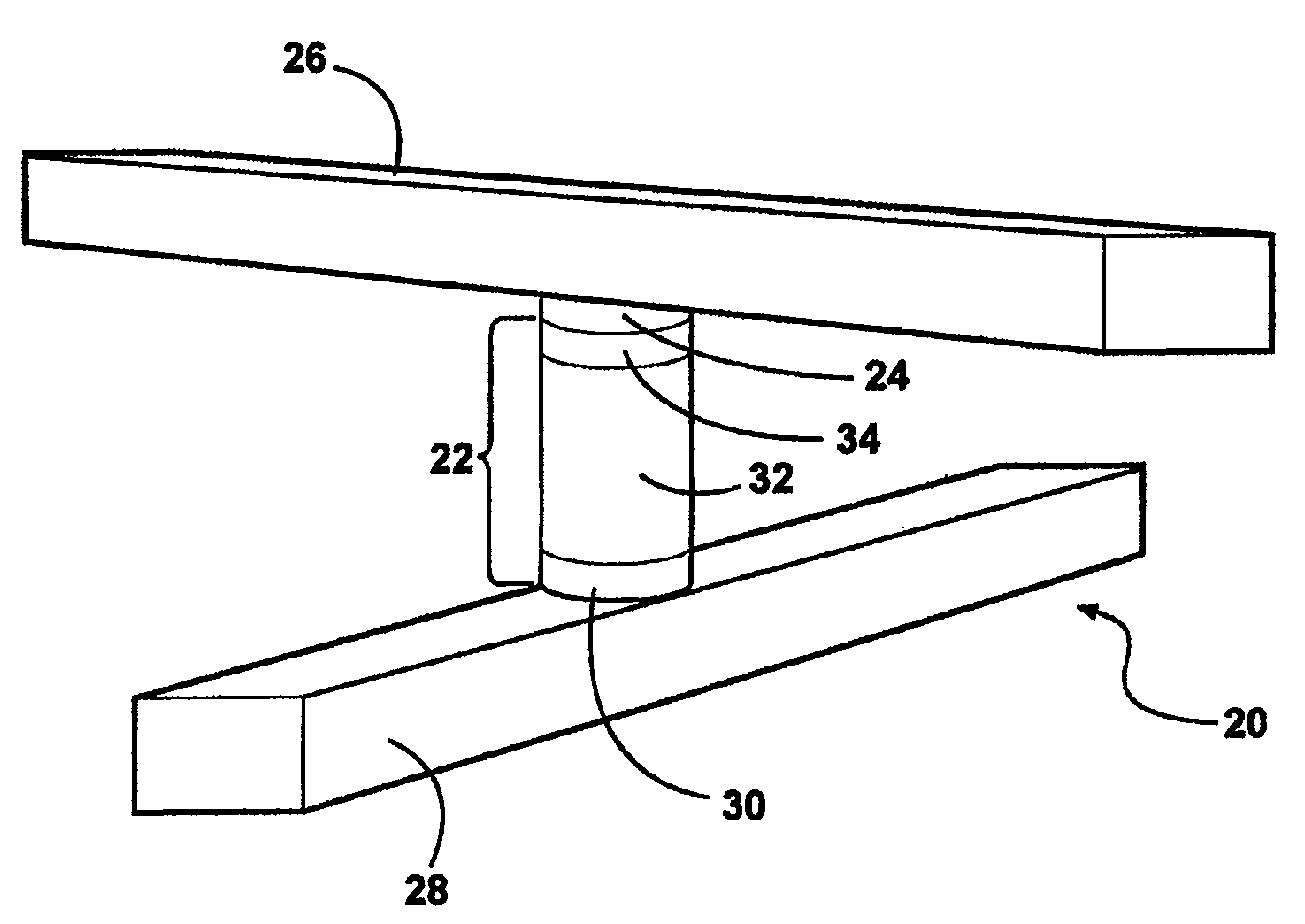
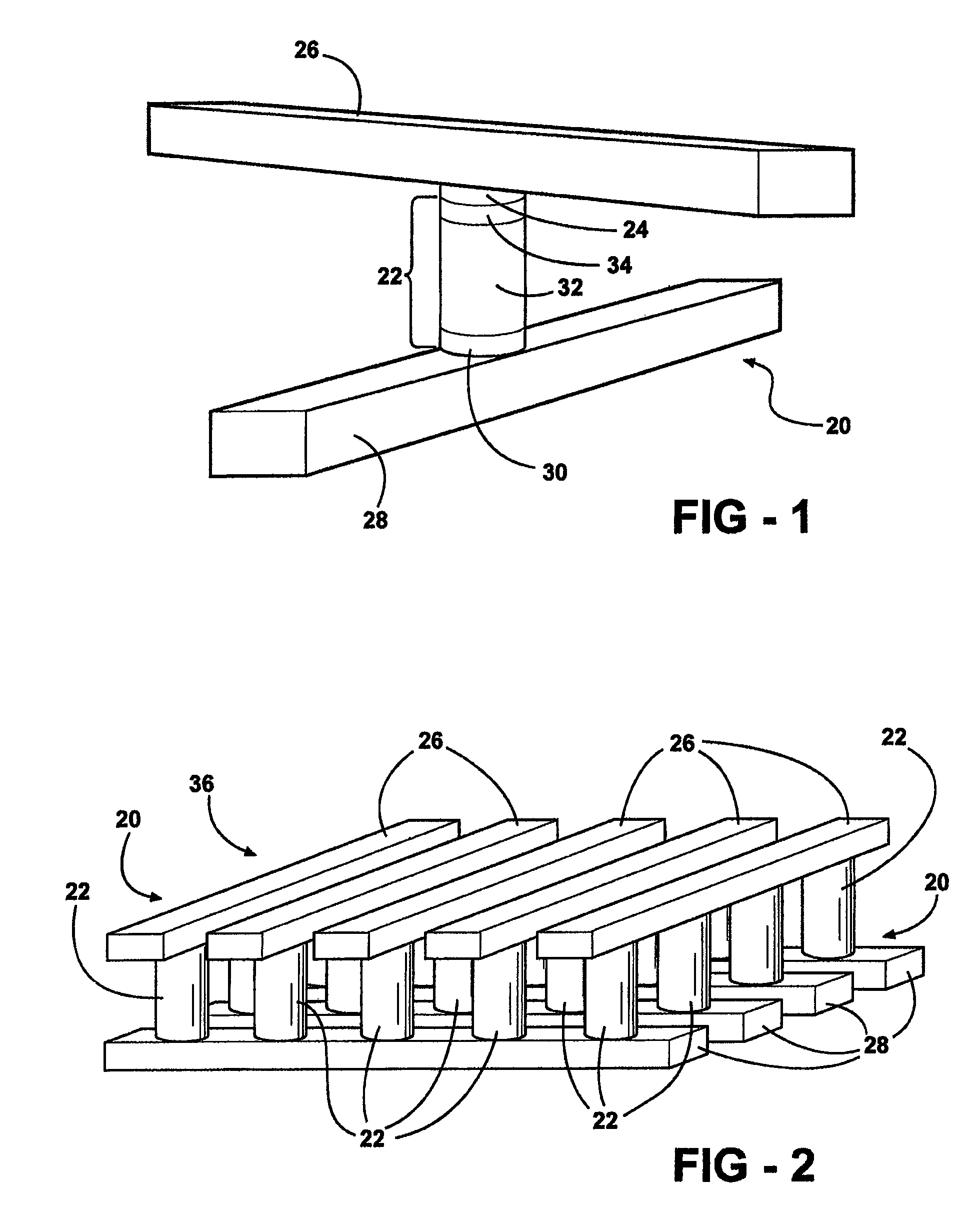
[0022]Referring to FIG. 1, U.S. Pat. No. 6,952,030, issued to Herner et al. and entitled “High-Density Three-Dimensional Memory Cell,” hereinafter the “'030 patent” and hereby incorporated by reference, discloses a nonvolatile memory cell, generally indicated at 20, including a vertically oriented junction diode 22 and a dielectric rupture antifuse 24 interposed between top 26 and bottom 28 conductors. The vertically oriented junction diode 22 includes a heavily doped semiconductor layer 30 of a first conductivity type, an intermediate layer 32 which is undoped semiconductor material or lightly doped semiconductor material, and a heavily doped semiconductor layer 34 of the second conductivity type. The semiconductor material of the junction diode 22 is generally silicon, germanium, or an alloy of silicon and / or germanium. The junction diode 22 and the dielectric rupture antifuse 24 are arranged in series between the bottom conductor 28 and the top conductor 26, which may be formed o...
PUM
 Abstract
Description
Claims
Application Information
 - R&D
- Intellectual Property
- Life Sciences
- Materials
- Tech Scout
- Unparalleled Data Quality
- Higher Quality Content
- 60% Fewer Hallucinations
Browse by: Latest US Patents, China's latest patents, Technical Efficacy Thesaurus, Application Domain, Technology Topic, Popular Technical Reports.
© 2025 PatSnap. All rights reserved.Legal|Privacy policy|Modern Slavery Act Transparency Statement|Sitemap|About US| Contact US: help@patsnap.com