Check patentability & draft patents in minutes with Patsnap Eureka AI!

Semiconductor memory device with high voltage generator

a memory device and high-voltage generator technology, applied in the direction of information storage, static storage, digital storage, etc., can solve the problems of voltage generation unit abnormal operation at high data clock frequency, irregular time interval between data packet arrival, etc., to prevent a drop of the level of external voltage and effective data window

Inactive Publication Date: 2010-03-30
SK HYNIX INC
View PDF24 Cites 4 Cited by
  • Summary
  • Abstract
  • Description
  • Claims
  • Application Information

AI Technical Summary

Benefits of technology

[0019]Embodiments of the present invention are directed to providing a high speed semiconductor memory device for preventing a drop of the level of an external voltage due to generation of high voltage to ensure an effective data window.

Problems solved by technology

When the duty cycle of the data clock DT_CLK is distorted, since data are irregularly transferred to the data pad, time intervals between data packet arrivals become irregular.
Due to the irregular time intervals, the size of an effective data window is reduced and the voltage generating unit abnormally operates at high data clock frequencies.

Method used


Image

  • Semiconductor memory device with high voltage generator
  • Semiconductor memory device with high voltage generator
  • Semiconductor memory device with high voltage generator

Examples


first embodiment

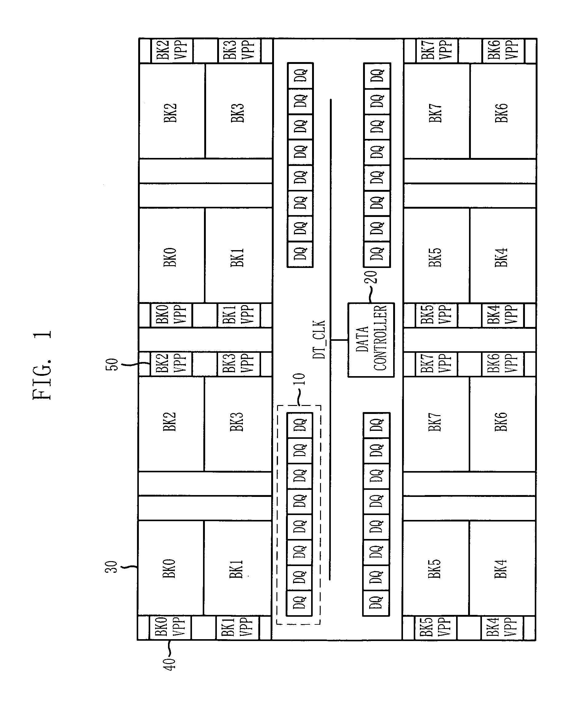
[0034]FIG. 4 is a block diagram illustrating a high voltage generator in a semiconductor memory device in accordance with the present invention.

[0035]Referring to FIG. 4, the high voltage generator includes a level detecting unit 100, a driving control unit 200, a first voltage generating unit 300, and a second voltage generating unit 400. The level detecting unit 100 detects a level of a high voltage VPP with respect to a reference voltage VREF to output a level detection signal PPEA. The driving control unit 200 receives the level detection signal PPEA and a refresh signal AREF to generate a driving control signal AREF_PPEA. The first voltage generating unit 300 generates the high voltage VPP by charge-pumping an external voltage VDD periodically in response to the driving control signal AREF_PPEA. The second voltage generating unit 400 generates the high voltage VPP by charge-pumping the external voltage VDD periodically in response to the level detection signal PPEA.

[0036]The fi...

second embodiment

[0048]FIG. 6 is a block diagram illustrating a high voltage generator in accordance with the present invention.

[0049]Referring to FIG. 6, the high voltage generator includes a level detecting unit 500, an oscillation signal generating unit 600, and a high voltage pumping unit 700. The level detecting unit 500 detects a level of a high voltage VPP with respect to a reference voltage VREF to output a level detection signal PPEA. The oscillation signal generating unit 600 generates an oscillation signal VPPOSC in response to the level detection signal PPEA, and adjusts a period of the oscillation signal VPPOSC in response to a refresh signal AREF. The high voltage pumping unit 700 generates a high voltage VPP having a voltage level higher than an external voltage VDD by charge-pumping the external voltage VDD during an activation period of the oscillation signal VPPOSC.

[0050]The high voltage generator in accordance with the second embodiment changes the period of the oscillation signal...


PUM


Abstract

A semiconductor memory device which prevents a drop of the level of an external voltage due to generation of high voltage, thereby ensuring an effective data window. The semiconductor memory device includes a level detecting unit and a voltage generating unit. The level detecting unit is configured to detect a level of an internal voltage based on a reference voltage to output a level detection signal. The voltage generating unit is configured to generate the internal voltage by selectively pumping an external voltage according to the level detection signal and a refresh signal.

Description

CROSS-REFERENCE TO RELATED APPLICATIONS[0001]This application claims priority to Korean patent application number 10-2007-0032051, filed on Mar. 31, 2007, which is incorporated by reference in its entirety.BACKGROUND OF THE INVENTION[0002]The subject matter relates to semiconductor design technology, and more particularly to a high speed semiconductor memory device for preventing a drop of the level of an external voltage due to generation of high voltage to thereby ensure an effective data window.[0003]FIG. 1 is a block diagram illustrating a conventional semiconductor memory device.[0004]Referring to FIG. 1, the semiconductor memory device includes a plurality of data pads 10, a data controller 20, a plurality of banks 30, and a plurality of high voltage generators 40 and 50. The data pads for a data input / output are disposed in a central region, each of which is composed by 8 bits. As illustrated the data pads are total 4 bytes. The data controller 20 receives an external voltage...

Claims


Application Information

Patent Timeline
Patent Type & Authority Patents(United States)
IPC IPC(8): G11C5/14
CPCG11C5/145G11C11/406G11C11/4074G11C29/021G11C29/028G11C5/14
Inventor JUNG, HO-DON
Owner SK HYNIX INC
Features
  • R&D
  • Intellectual Property
  • Life Sciences
  • Materials
  • Tech Scout
  • Unparalleled Data Quality
  • Higher Quality Content
  • 60% Fewer Hallucinations
Learn More