Supercharge Your Innovation With Domain-Expert AI Agents!

High voltage transistors

a high-voltage transistor and transistor technology, applied in the field of semiconductor devices, can solve the problems of sub-threshold leakage current, device high breakdown voltage for high-voltage operation, and possible production of great leakage curren

Active Publication Date: 2010-04-27
SAMSUNG ELECTRONICS CO LTD
View PDF13 Cites 5 Cited by
  • Summary
  • Abstract
  • Description
  • Claims
  • Application Information

AI Technical Summary

Problems solved by technology

When driven at a high voltage, these devices may have high breakdown voltages for the operation at the high voltage.
The hump caused by the parasitic transistor possibly produces a great leakage current.
The parasitic transistor may result in a sub-threshold leakage current in some excessive cases.

Method used


Image

  • High voltage transistors
  • High voltage transistors
  • High voltage transistors

Examples


Embodiment Construction

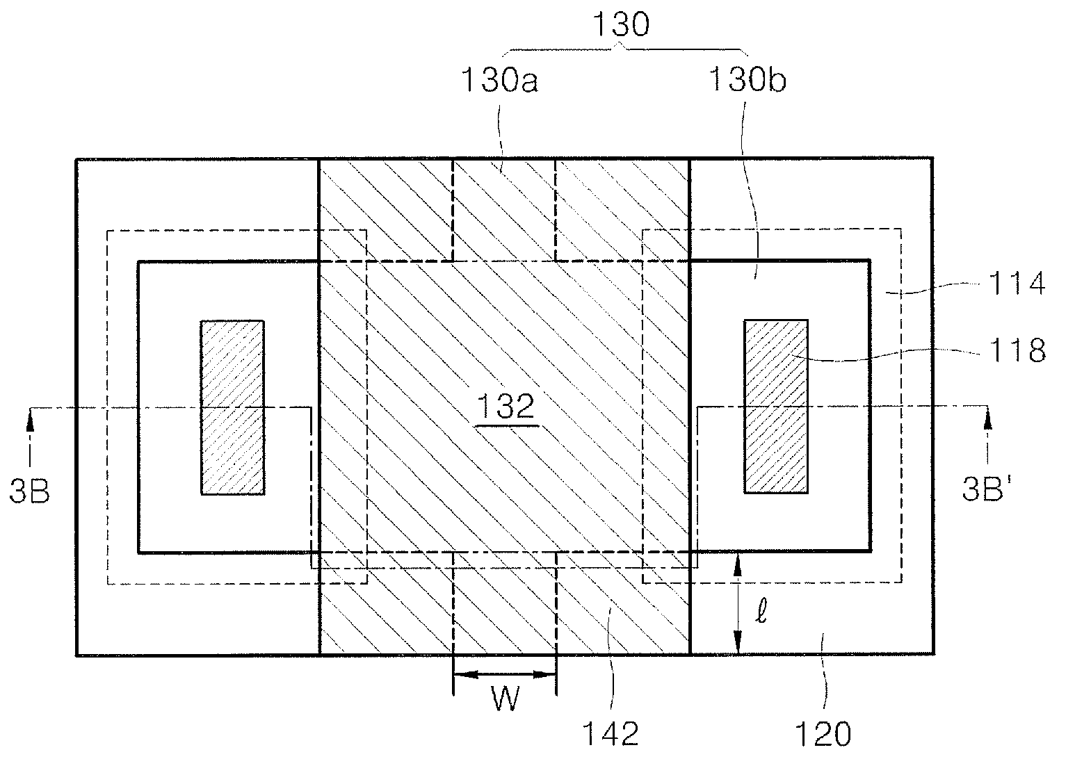
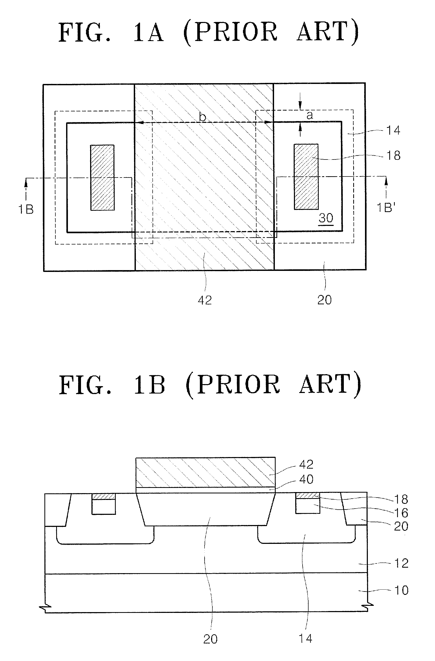
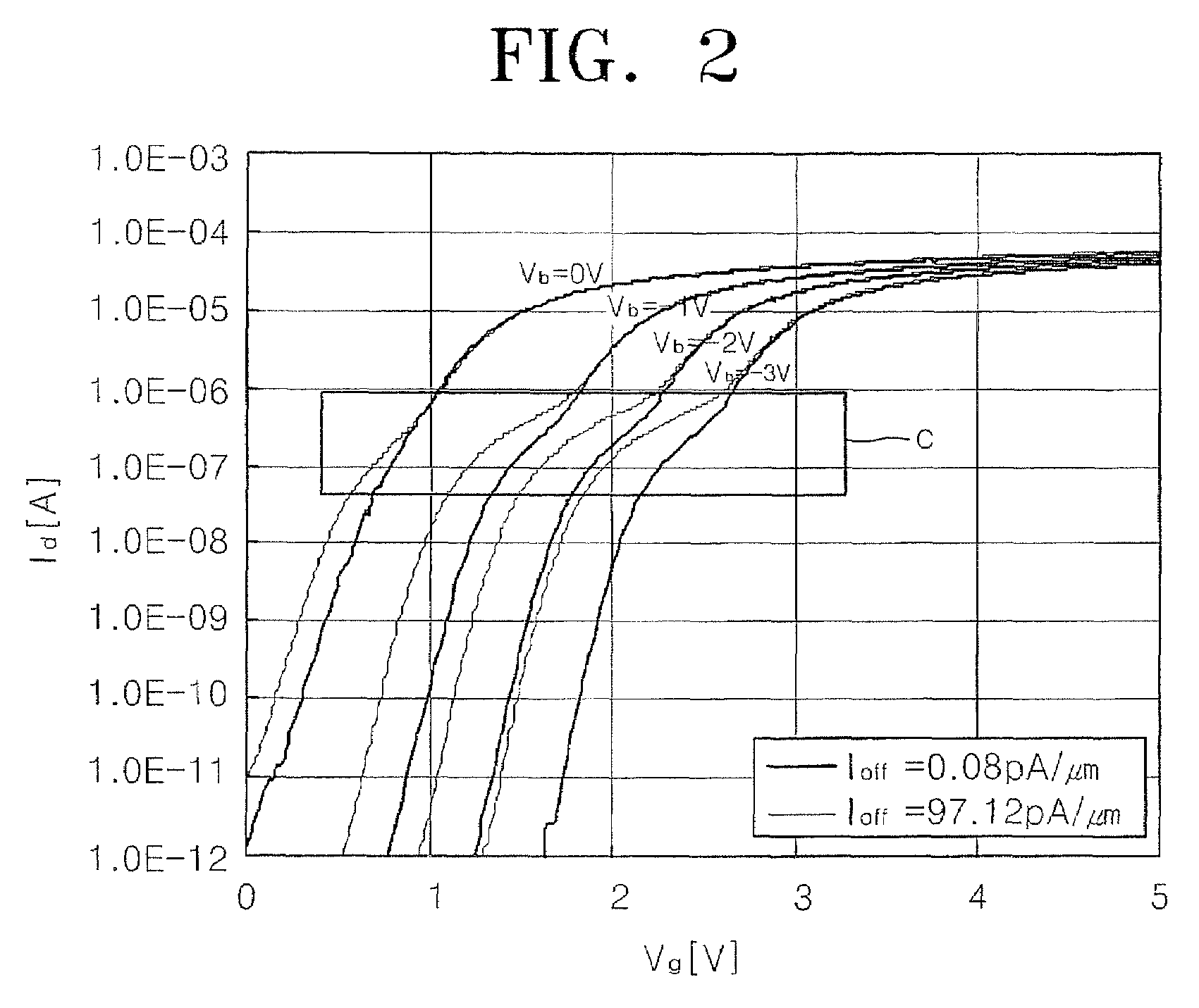
[0027]The invention is described more fully hereinafter with reference to the accompanying drawings, in which embodiments of the invention are shown. This invention may, however, be embodied in many different forms and should not be construed as limited to the embodiments set forth herein. Rather, these embodiments are provided so that this disclosure will be thorough and complete, and will fully convey the scope of the invention to those skilled in the art. In the drawings, the size and relative sizes of layers and regions may be exaggerated for clarity.

[0028]It will be understood that when an element or layer is referred to as being “on,”“connected to” or “coupled to” another element or layer, it can be directly on, connected or coupled to the other element or layer or intervening elements or layers may be present. In contrast, when an element is referred to as being “directly on,”“directly connected to” or “directly coupled to” another element or layer, there are no intervening e...


PUM


Abstract

Some embodiments of the present invention provide high voltage transistors including a semiconductor substrate and a device isolation film defining an active region in the semiconductor substrate. A gate electrode extends along a central portion of the active region while maintaining a predetermined width on the semiconductor substrate. A second well is formed on both sides of the gate electrode in the semiconductor substrate, and partially extends to a bottom surface of the device isolation film. The active region in the semiconductor substrate comprises a first active region disposed under the gate electrode, and separating the device isolation film and a second active region defined by the first active region and the device isolation film. Methods of manufacturing high voltage transistors are also provided.

Description

CLAIM OF PRIORITY[0001]This application claims priority under 35 U.S.C. §119 to Korean Patent Application No. 10-2007-0011251, filed on Feb. 2, 2007 in the Korean Intellectual Property Office (KIPO), the content of which is hereby incorporated herein by reference as if set forth in its entirety.FIELD OF THE INVENTION[0002]The present invention relates to a semiconductor devices and methods of manufacturing the same, and more particularly to, high voltage transistors and methods of manufacturing the sameBACKGROUND OF THE INVENTION[0003]Complementary metal oxide silicon (CMOS) driven at low voltages and logic element devices driven at high voltages can be combined on a single semiconductor substrate. When driven at a high voltage, these devices may have high breakdown voltages for the operation at the high voltage. In order to obtain the high breakdown voltage, a density of an impurity doped into a well formed in the semiconductor substrate is typically decreased.[0004]Referring to FI...

Claims


Application Information

Patent Timeline
Patent Type & Authority Patents(United States)
IPC IPC(8): H01L29/78
CPCH01L29/0653H01L29/78H01L29/66568H01L29/0692H01L29/42368H01L29/6659H01L29/7833
Inventor KWON, OH-KYUMKIM, YONG-CHANOH, JOON-SUKKIM, MYUNG-HEEPARK, HYE-YOUNG
Owner SAMSUNG ELECTRONICS CO LTD
Features
  • R&D
  • Intellectual Property
  • Life Sciences
  • Materials
  • Tech Scout
  • Unparalleled Data Quality
  • Higher Quality Content
  • 60% Fewer Hallucinations
Learn More