Method of mounting a semiconductor chip
a technology of semiconductor chips and mounting methods, which is applied in the direction of semiconductor/solid-state device details, soldering apparatus, manufacturing tools, etc., can solve the problems of ineffective bonding strength of bonded parts, complex circuit board construction, and simple insertion of protruding patterns at the positions of bonded bumps, so as to increase the bonding strength and improve the bonding strength
- Summary
- Abstract
- Description
- Claims
- Application Information
AI Technical Summary
Benefits of technology
Problems solved by technology
Method used
Image

Examples
first embodiment
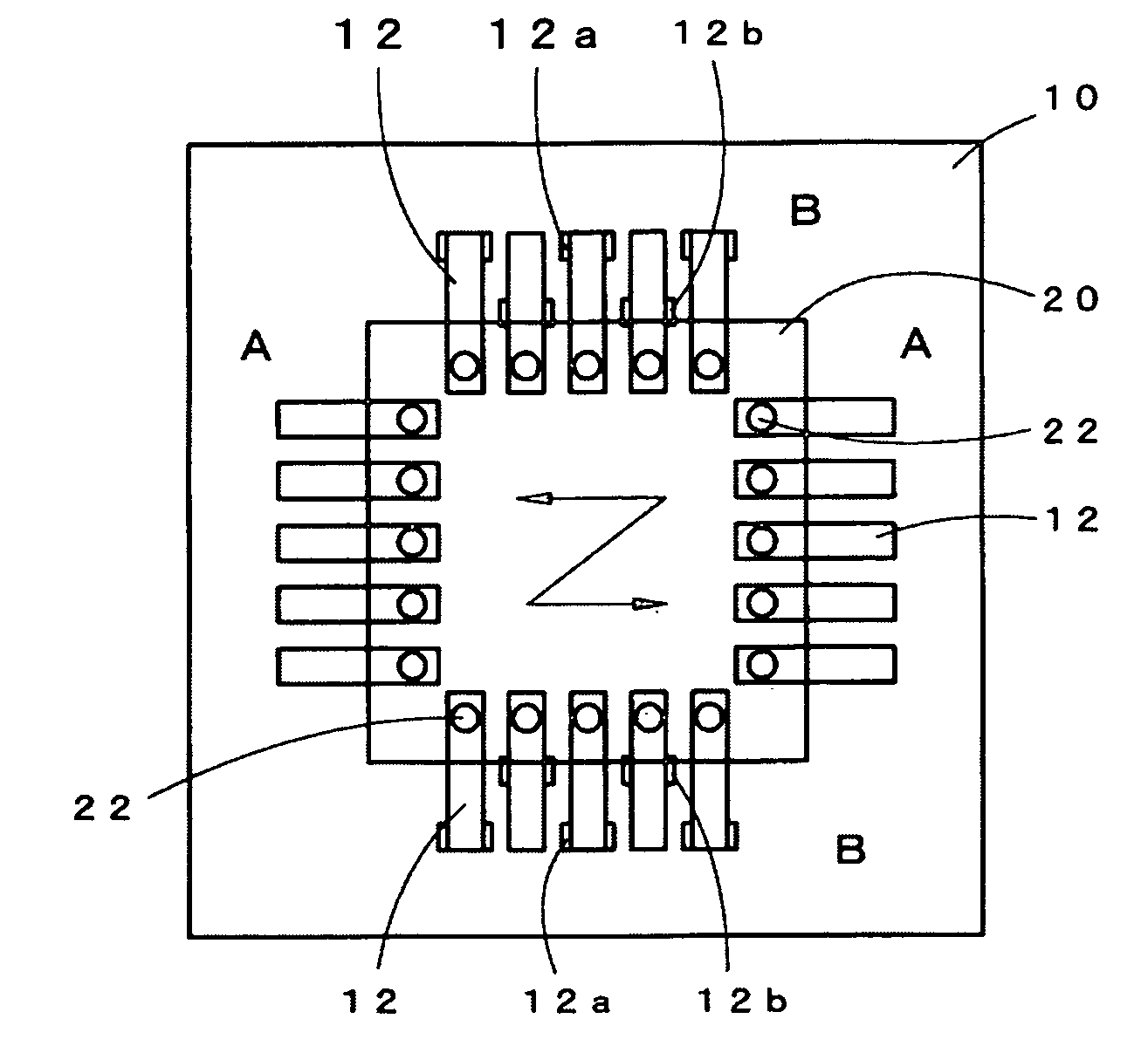
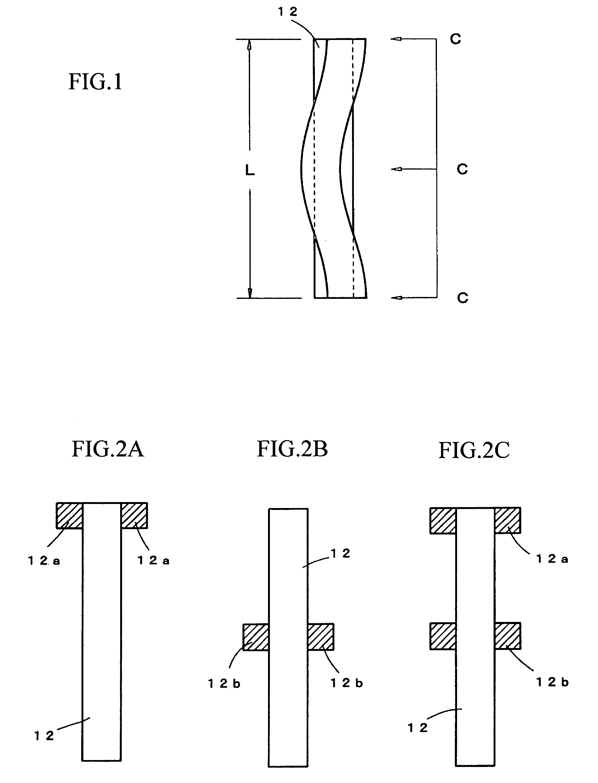
[0031]FIGS. 1 to 3 show a first embodiment of the method of mounting a semiconductor chip according to the present invention. FIG. 1 shows, as an example of one bonding pattern 12 formed on a circuit board, a state where ultrasonic vibration is applied to a bonding pattern 12 so that the direction of vibration is perpendicular to the longitudinal direction of the bonding pattern 12. In the same way as the bonding patterns 12 in part B of the circuit board 10 shown in FIG. 6 as the conventional art, the bonding pattern 12 in FIG. 1 is formed with a long narrow planar form.
[0032]When ultrasonic vibration is applied to the bonding pattern 12 with the direction of vibration perpendicular to the longitudinal direction of the bonding pattern 12 and the bonding pattern 12 resonates, both ends of the bonding pattern 12 in the longitudinal direction inevitably become antinodes of vibration. FIG. 1 shows the case where antinodes of vibration (C points) are produced at both ends and the center...
second embodiment
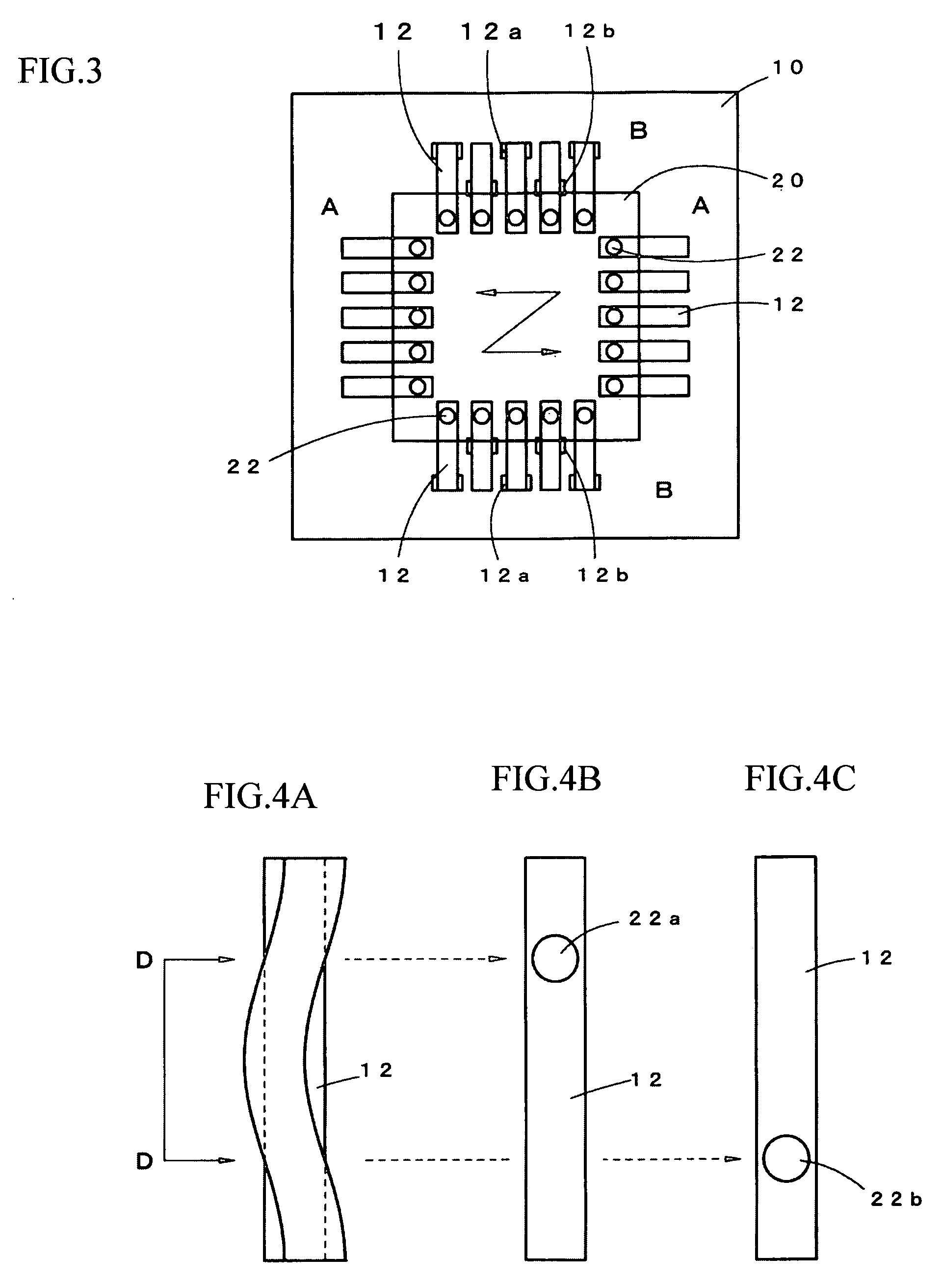
[0043]FIGS. 4 and 5 show a second embodiment of the method of mounting a semiconductor chip according to the present invention.
[0044]FIG. 4A shows a state where ultrasonic vibration is applied to a bonding pattern 12 resulting in the bonding pattern 12 resonating. The D points in FIG. 4A show the positions of the nodes in the state where the bonding pattern 12 resonates. It should be noted that in the illustrated example, the length L of the bonding pattern 12 corresponds to one wavelength.
[0045]In the method of mounting a semiconductor chip according to the present embodiment, when ultrasonic vibration is applied to the semiconductor chip 20 to mount the semiconductor chip 20 to the circuit board 10 by flip-chip bonding, the semiconductor chip 20 is mounted so that the bonding positions of the bumps 22 provided on the semiconductor chip 20 are positioned at the positions (D points) of the nodes when the bonding pattern 12 resonates. That is, for the example of the resonance shown i...
third embodiment
[0049]When applying ultrasonic vibration to the semiconductor chip 20 to mount the semiconductor chip 20 on the circuit board 10, the third embodiment of the method of mounting the semiconductor chip according to the present invention mounts the semiconductor chip 20 by setting the lengths, pattern widths, and pattern heights of the bonding patterns 12 so that the bonding patterns 12 do not resonate due to the ultrasonic vibration.
[0050]As one example, if a bonding pattern 12 is shaped so as to be rectangular in planar form as shown in FIG. 1, when the bonding pattern 12 resonates due to the application of ultrasonic vibration in a direction perpendicular to the longitudinal direction of the bonding pattern 12, mounting is carried out with the length L of the bonding pattern 12 set at (λ / 2)×(n+1 / 2) so as to suppress resonance of the bonding pattern 12. It should be noted that n is an integer and λ is the wavelength of the resonant frequency.
[0051]Since the bonding patterns 12 have a...
PUM
| Property | Measurement | Unit |
|---|---|---|
| area | aaaaa | aaaaa |
| bonding strength | aaaaa | aaaaa |
| strength | aaaaa | aaaaa |
Abstract
Description
Claims
Application Information
 - R&D
- Intellectual Property
- Life Sciences
- Materials
- Tech Scout
- Unparalleled Data Quality
- Higher Quality Content
- 60% Fewer Hallucinations
Browse by: Latest US Patents, China's latest patents, Technical Efficacy Thesaurus, Application Domain, Technology Topic, Popular Technical Reports.
© 2025 PatSnap. All rights reserved.Legal|Privacy policy|Modern Slavery Act Transparency Statement|Sitemap|About US| Contact US: help@patsnap.com