Supercharge Your Innovation With Domain-Expert AI Agents!

Substrate processing method, photomask manufacturing method, photomask, and device manufacturing method

a technology of substrate processing and manufacturing method, applied in the direction of photomechanical treatment, instruments, electrical devices, etc., can solve the problems of difficult control of etching rate when compared with aluminum, and the speed of the operation of the devi

Active Publication Date: 2010-05-11
NIKON CORP
View PDF23 Cites 10 Cited by
  • Summary
  • Abstract
  • Description
  • Claims
  • Application Information

AI Technical Summary

Benefits of technology

[0018]According to this method, the device linewidth characteristic is predicted based on the sharp-edged feature of the projected image of the predetermined pattern, and based on the device linewidth characteristic that has been predicted, the exposure condition of the pattern is adjusted. Accordingly, by performing exposure under the adjusted exposure condition, or in other words, by performing patterning of the resist coated on the substrate (or on the thin film on the substrate) with the projected image of the pattern and developing the substrate after the patterning, a resist pattern that satisfies the desired device linewidth characteristic is formed on the substrate (or on the thin film on the substrate). In the manner described above, it becomes possible to form a pattern of a desired linewidth on the substrate.
[0021]According to this method, in the substrate processing step, because the pattern is formed on the substrate using the substrate processing method of the present invention, a pattern of a desired linewidth can be formed on the substrate, which can suppress the generation of unevenness and variation in the finished size of the device, and a device with a good operation speed can be manufactured with good yield.
[0025]According to this method, the device linewidth characteristic is predicted based on the sharp-edged feature of the projected image of the pattern that is to be formed on the photomask, and the linewidth is changed in at least a part of the pattern based on the device linewidth characteristic that has been predicted, and the pattern whose linewidth in a part of the pattern has been changed is formed on the mask substrate. Accordingly, by performing exposure using the photomask manufactured in the manner described above, or in other words, by performing patterning of the resist coated on the substrate (or on the thin film on the substrate) with the projected image of the pattern and developing the substrate after the patterning, a resist pattern that satisfies the desired device linewidth characteristic is formed on the substrate (or on the thin film on the substrate). In the manner described above, it becomes possible to form a pattern of a desired linewidth on the substrate.

Problems solved by technology

However, with copper, a technique referred to as the damascene method is employed as the technique for forming wiring without etching the copper (refer to, for example, Kokai (Japanese Patent Unexamined Application Publication) No. 2002-270586), taking into consideration the fact that etching rate control is difficult when compared with aluminum.
Because unevenness or variation in the finished dimension of devices particularly affects the yield or the operation speed of the device, requirements to reduce unevenness and variation are pressing.

Method used


Image

  • Substrate processing method, photomask manufacturing method, photomask, and device manufacturing method
  • Substrate processing method, photomask manufacturing method, photomask, and device manufacturing method
  • Substrate processing method, photomask manufacturing method, photomask, and device manufacturing method

Examples


Embodiment Construction

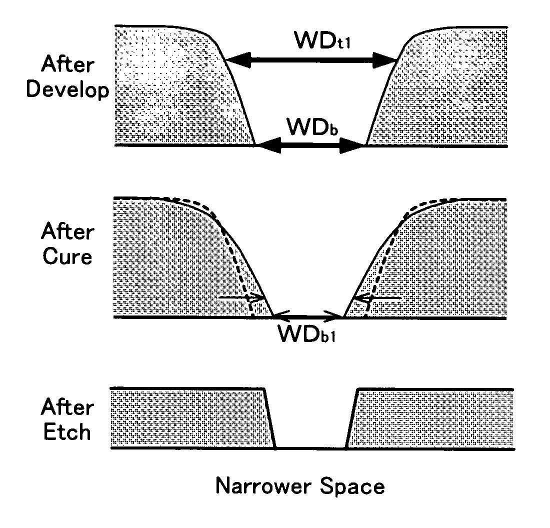
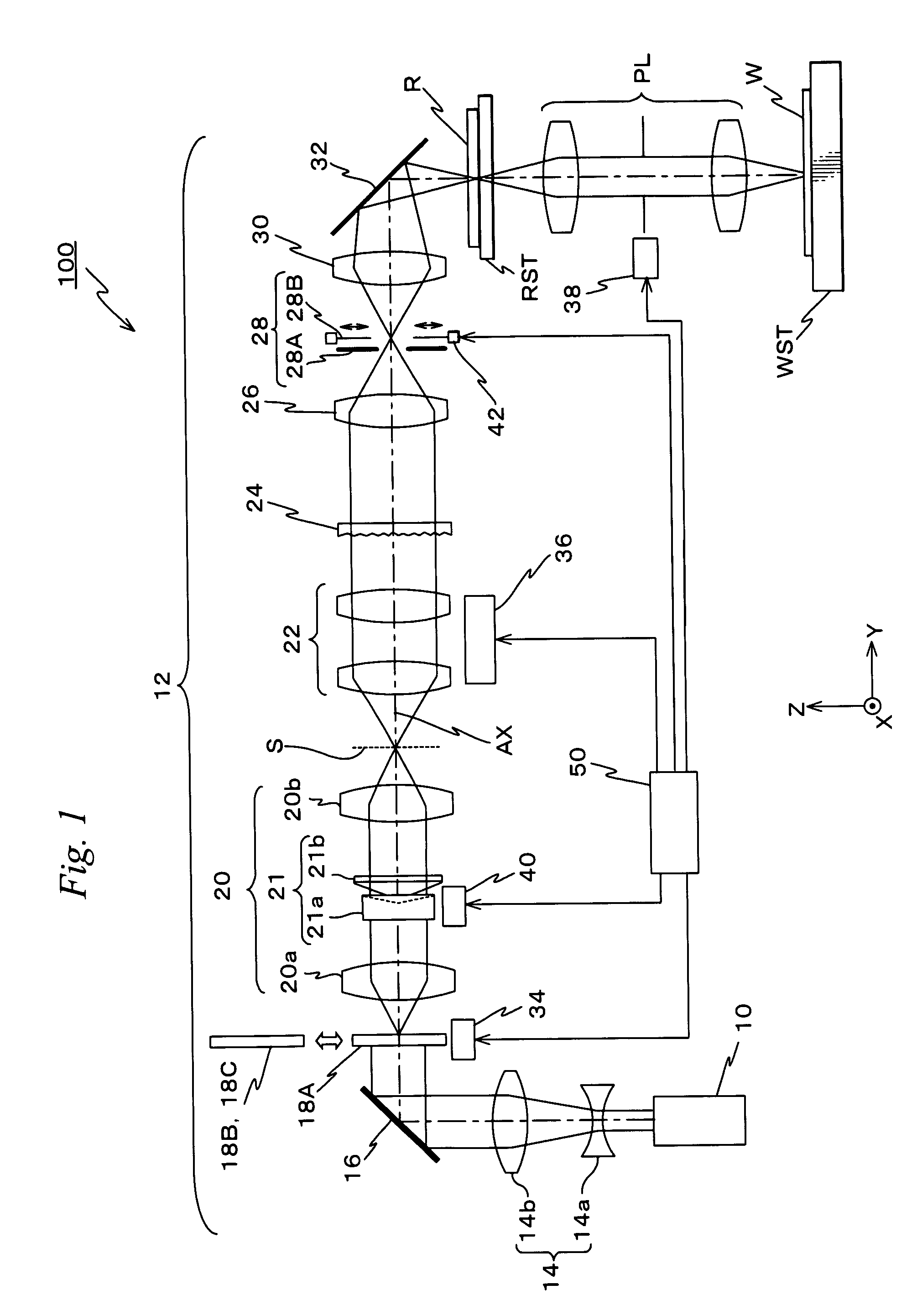
[0037]Hereinafter, a first embodiment of the present invention will be described, based on FIGS. 1 to 7B. FIG. 1 shows an entire view of an arrangement of an exposure apparatus 100 related to the first embodiment. Exposure apparatus 100 is a scanning exposure apparatus based on a step-and-scan method, that is, the so-called scanning stepper (also called a scanner). In FIG. 1, a Z-axis is set parallel to a single optical axis AX of a projection optical system PL, a Y-axis is set in a direction parallel to the page surface of FIG. 1 within a plane orthogonal to the Z-axis, and an X-axis is set in a direction perpendicular to the page surface of FIG. 1. In FIG. 1, an illumination optical system 12 which will be described later is set to perform an annular illumination.

[0038]The exposure apparatus in FIG. 1 is provided with an illumination system that includes a light source 10 and illumination optical system 12, a reticle stage RST on which a reticle (photomask) R is mounted, projectio...


PUM


Abstract

A device linewidth characteristic is predicted based on a sharp-edged feature of a projected image of a predetermined pattern (steps 104 to 110), and an exposure condition of the pattern is adjusted based on the device linewidth characteristic that has been predicted (step 112). Then, exposure is performed under the adjusted exposure condition. That is, patterning of a resist on a substrate is performed with the projected image of the pattern (step 114). And, by developing the substrate after patterning, a resist pattern that satisfies a desired device linewidth characteristic is formed on the substrate. Accordingly, by performing etching of the substrate with the resist pattern serving as a mask, a pattern after etching can be formed with a desired linewidth.

Description

CROSS-REFERENCE TO RELATED APPLICATIONS[0001]This non-provisional application claims the benefit of Provisional Application No. 60 / 772,879 filed Feb. 14, 2006, the disclosure of which is hereby incorporated herein by reference in its entirety.BACKGROUND OF THE INVENTION[0002]1. Field of the Invention[0003]The present invention relates to substrate processing methods, manufacturing method of photomasks, photomasks, and device manufacturing methods, and more particularly to a substrate processing method that includes a patterning step in which patterning of a resist on a substrate is performed by exposure for manufacturing electronic devices (microdevices) such as a semiconductor, a manufacturing method of a photomask used in the patterning step, a photomask manufactured by the manufacturing method, and a device manufacturing method that uses the substrate processing method or the photomask.[0004]2. Description of the Background Art[0005]When manufacturing electronic devices, in the s...

Claims


Application Information

Patent Timeline
Patent Type & Authority Patents(United States)
IPC IPC(8): H01L21/00
CPCG03F1/144G03F7/705G03F7/70108G03F1/36
Inventor HIRUKAWA, SHIGERU
Owner NIKON CORP
Features
  • R&D
  • Intellectual Property
  • Life Sciences
  • Materials
  • Tech Scout
  • Unparalleled Data Quality
  • Higher Quality Content
  • 60% Fewer Hallucinations
Learn More