Singulation method of semiconductor device
a semiconductor device and semiconductor technology, applied in the field of semiconductor device manufacturing, can solve problems such as yield reduction, and achieve the effect of stable separation of chips
- Summary
- Abstract
- Description
- Claims
- Application Information
AI Technical Summary
Benefits of technology
Problems solved by technology
Method used
Image

Examples
Embodiment Construction
[0031]Reference will now be made in detail to the embodiments of the present disclosure, examples of which are illustrated in the accompanying drawings.
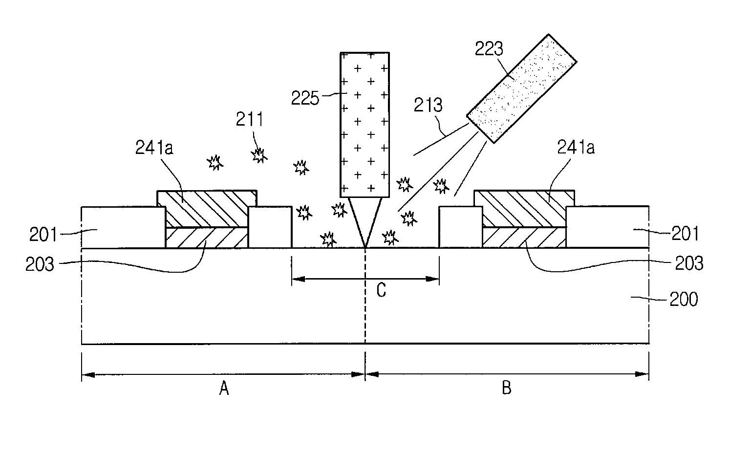
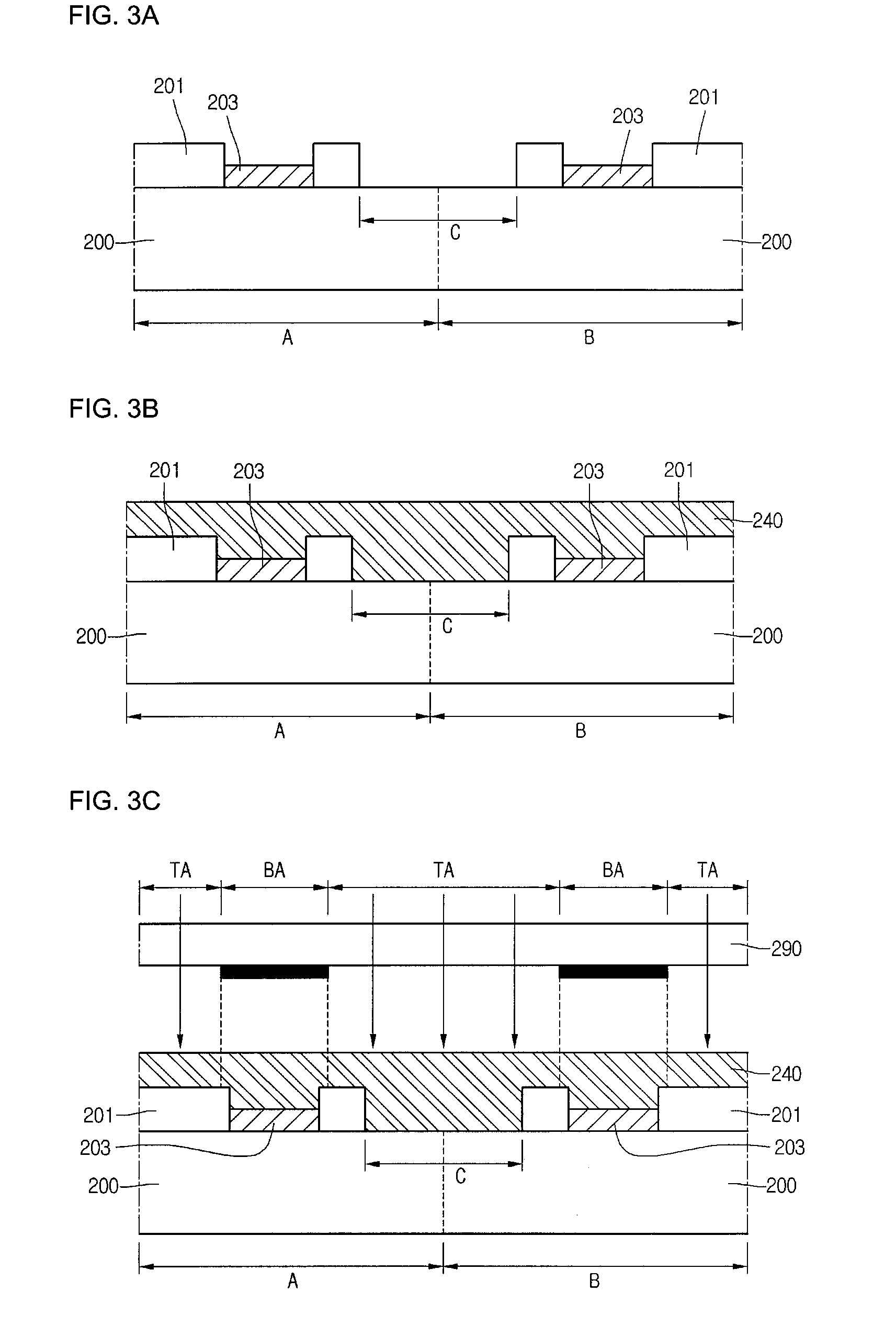
[0032]FIGS. 3A to 3G are sectional views illustrating a manufacturing process of a semiconductor device according to the present disclosure.
[0033]A first wafer A and a second wafer B include a scribe lane region C and a semiconductor chip region in which a semiconductor chip is formed.
[0034]First wafer A and second wafer B are separated into individual wafers by a sawing process after a semiconductor device forming process.
[0035]A plurality of semiconductor devices such as transistors, wiring structures between the transistors, and interlayer insulating layers for insulating between devices are formed in each semiconductor chip region of first wafer A and second wafer B.
[0036]Referring to FIG. 3A, a metal pad 203 is formed on a semiconductor substrate 200 of first wafer A and second wafer B.
[0037]For example, the metal pad 203 can be...
PUM
 Abstract
Description
Claims
Application Information
 - R&D
- Intellectual Property
- Life Sciences
- Materials
- Tech Scout
- Unparalleled Data Quality
- Higher Quality Content
- 60% Fewer Hallucinations
Browse by: Latest US Patents, China's latest patents, Technical Efficacy Thesaurus, Application Domain, Technology Topic, Popular Technical Reports.
© 2025 PatSnap. All rights reserved.Legal|Privacy policy|Modern Slavery Act Transparency Statement|Sitemap|About US| Contact US: help@patsnap.com