Supercharge Your Innovation With Domain-Expert AI Agents!

Configurable polishing apparatus

a technology of polishing apparatus and configuration, which is applied in the direction of grinding drive, lapping machine, manufacturing tools, etc., can solve the problems of cmp equipment and inability to perform three-step serial cmp processes

Inactive Publication Date: 2010-08-17
HAM THOMAS H
View PDF8 Cites 5 Cited by
  • Summary
  • Abstract
  • Description
  • Claims
  • Application Information

AI Technical Summary

Benefits of technology

Enables the flexible execution of various multi-step CMP processes, from two to three or more steps, by expanding the polishing capacity without requiring new equipment, thus enhancing the versatility and efficiency of semiconductor wafer fabrication.

Problems solved by technology

For example, a CMP equipment with two serially arranged polishing stations, which is designed for two-step serial CMP processes, cannot perform three-step serial CMP processes.

Method used


Image

  • Configurable polishing apparatus
  • Configurable polishing apparatus
  • Configurable polishing apparatus

Examples


Embodiment Construction

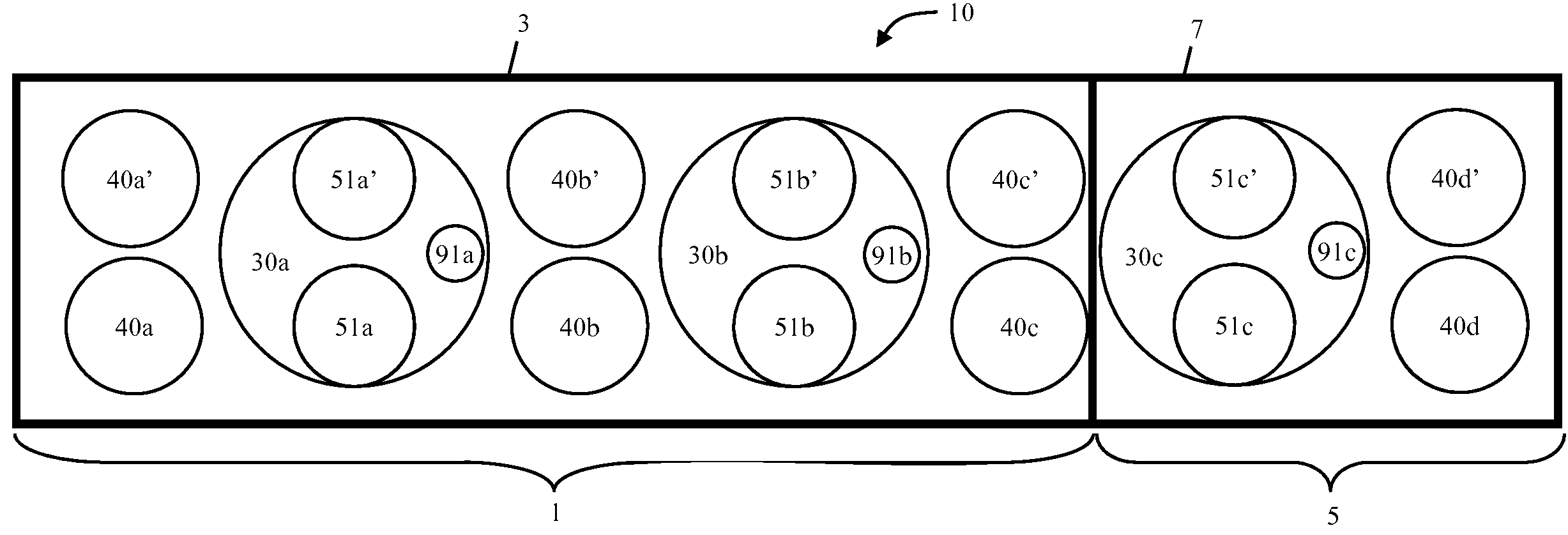
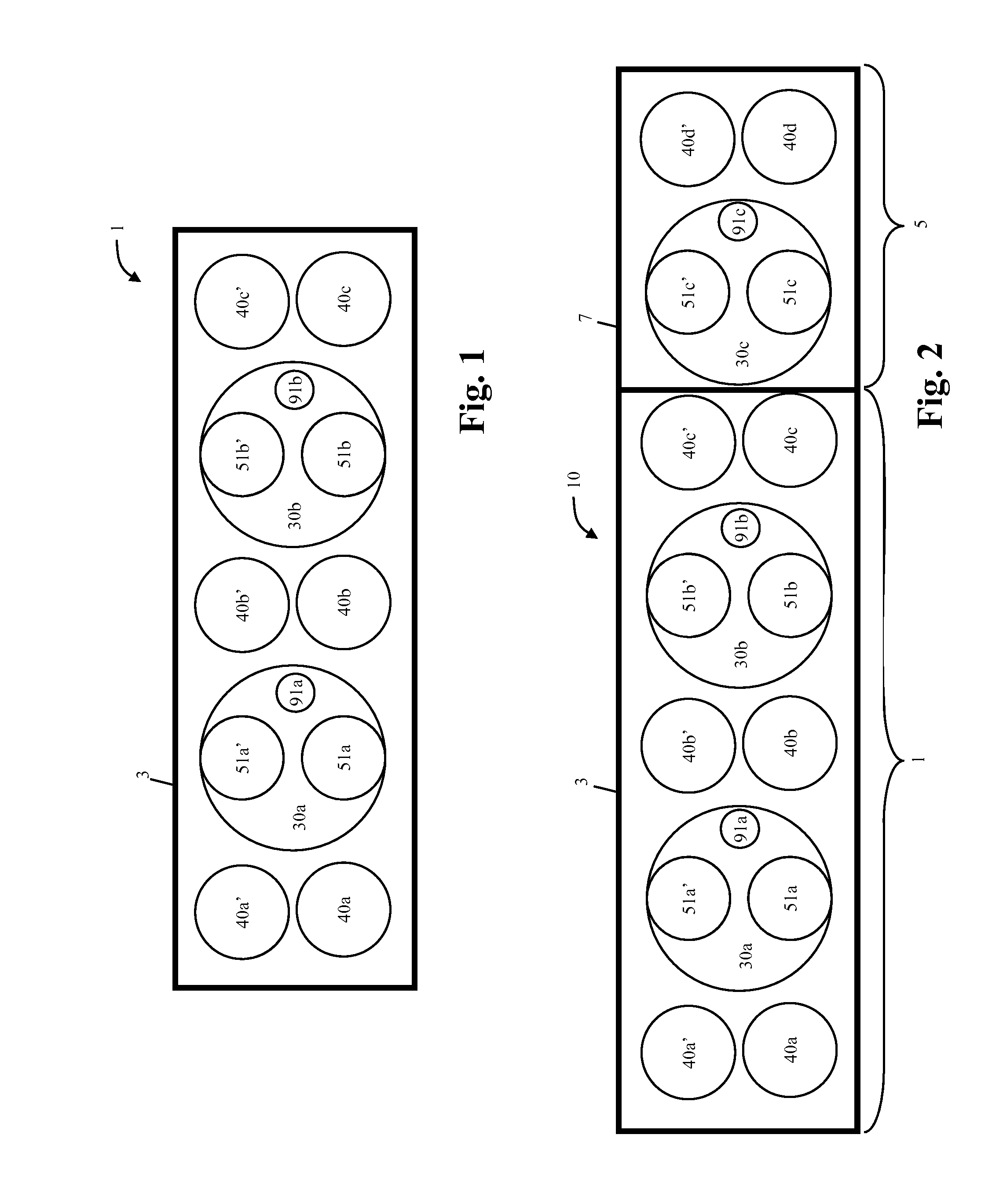
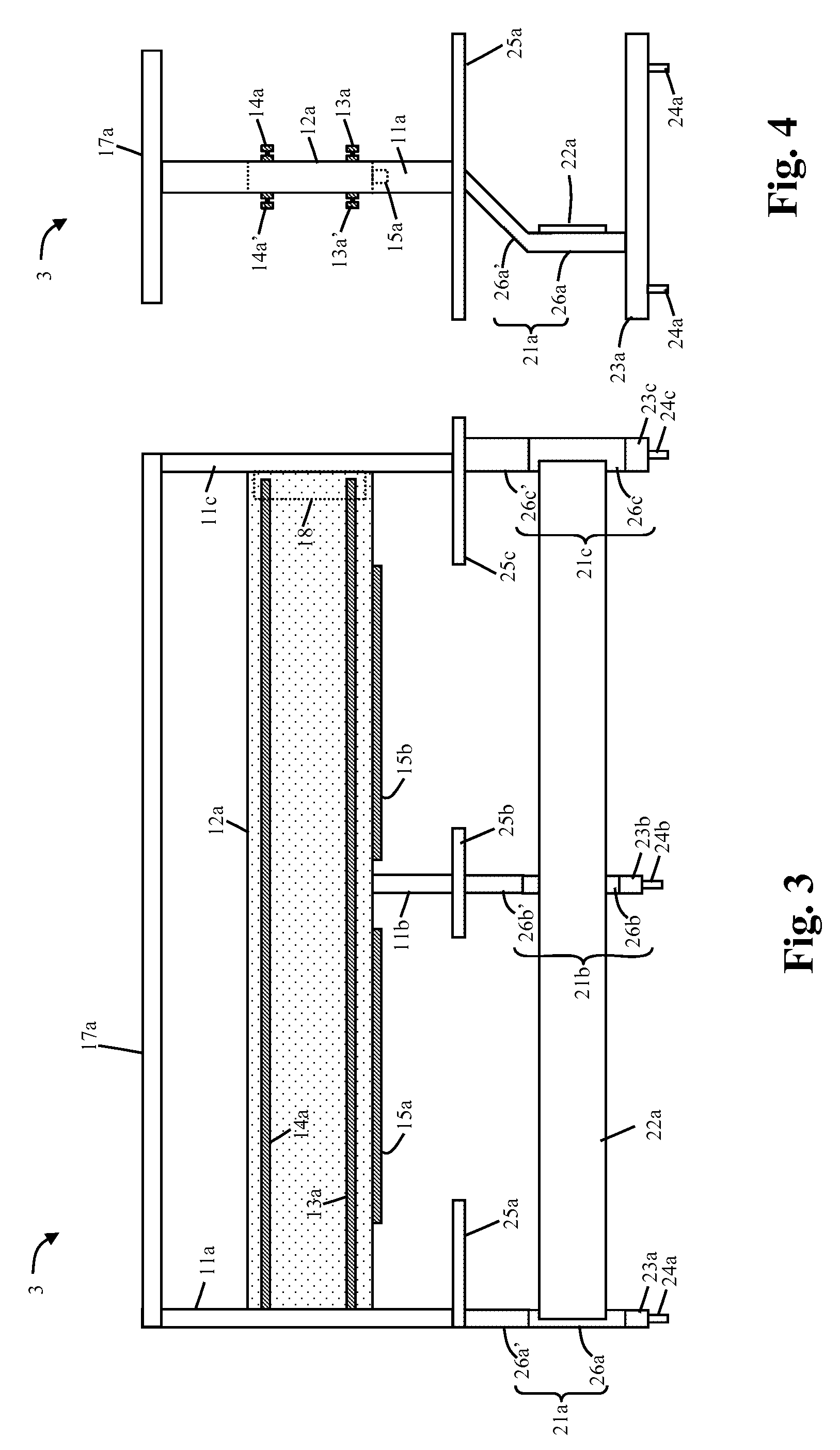
[0021]With reference of FIG. 1, a polishing apparatus 1 in accordance with an embodiment of the invention is described. The polishing apparatus 1 comprises polishing tables 30a and 30b, load-and-unload stations 40a, 40a′, 40b, 40b′, 40c and 40c′, polishing heads 51a, 51a′, 51b and 51b′, and a frame structure 3, which is generally indicated as a rectangle in FIG. 1. The polishing tables 30a and 30b, the load-and-unload stations 40a, 40a′, 40b, 40b′, 40c and 40c′, and the polishing or carrier heads 51a, 51a′, 51b and 51b′ are directly or indirectly attached to the frame structure 3. The frame structure 3 is described in more detail below with reference to FIGS. 3 and 4.

[0022]As shown in FIG. 1, the polishing tables 30a and 30b and the load-and-unload stations 40a, 40a′, 40b, 40b′, 40c and 40c′ are attached to the frame structure 3 such that the first polishing table 30a is situated between the first and second load-and-unload stations 40a and 40a′ and the third and fourth load-and-unl...


PUM

PropertyMeasurementUnit
torqueaaaaaaaaaa
electrical currentaaaaaaaaaa
shapeaaaaaaaaaa

Abstract

A polishing apparatus for polishing semiconductor wafers comprises a main polishing structure, which includes a plurality of polishing tables, a plurality of polishing heads and a plurality of load-and-unload stations, and an add-on polishing structure, which includes an additional polishing table and an additional polishing head. The add-on polishing structure can be attached to the main polishing structure to form a larger polishing structure with the additional polishing table and the additional polishing head.

Description

CROSS REFERENCE TO RELATED APPLICATION[0001]This application is entitled to the benefit of U.S. Provisional Patent Application Ser. Nos. 60 / 813,498, filed on Jun. 14, 2006, 60 / 830,472, filed on Jul. 13, 2006, and 60 / 844,578, filed on Sep. 13, 2006, which are incorporated herein by reference.FIELD OF THE INVENTION[0002]The invention relates generally to semiconductor processing equipments, and more particularly to a polishing apparatus.BACKGROUND OF THE INVENTION[0003]Chemical mechanical polishing (CMP) process is widely used for planarization during fabrication of semiconductor devices. In general, CMP process involves polishing a surface of a semiconductor wafer on a polishing surface, e.g., a polishing pad, using a solution, e.g., a slurry solution, supplied between the wafer surface and the polishing surface. Depending on the CMP process, multiple CMP steps may be performed to produce a single planarized layer on the semiconductor wafer. As an example, multiple CMP steps may be p...

Claims


Application Information

Patent Timeline
Patent Type & Authority Patents(United States)
IPC IPC(8): B24B49/00B24B51/00
CPCB24B37/12B24B37/345
Inventor JEONG, IN-KWONBERKSTRESSER, DAVID E.
Owner HAM THOMAS H
Features
  • R&D
  • Intellectual Property
  • Life Sciences
  • Materials
  • Tech Scout
  • Unparalleled Data Quality
  • Higher Quality Content
  • 60% Fewer Hallucinations
Learn More