Check patentability & draft patents in minutes with Patsnap Eureka AI!

Semiconductor memory apparatus

a memory apparatus and semiconductor technology, applied in the field of semiconductor memory apparatus, can solve the problems of preventing the realization of high speed operation and high integration, affecting the stability of the corresponding data input circuit, etc., and achieve the effect of improving area efficiency and ensuring stability

Active Publication Date: 2010-11-02
SK HYNIX INC
View PDF14 Cites 2 Cited by
  • Summary
  • Abstract
  • Description
  • Claims
  • Application Information

AI Technical Summary

Benefits of technology

[0011]A semiconductor memory apparatus capable of securing stability and improving area efficiency in a data input operation is described herein.

Problems solved by technology

Moreover, since timing differences between internal clock signals transmitted to respective data input buffers during high speed operations require detailed attention compared to low speed operations, operational stability in a corresponding data input circuit has become degraded.
As a result, a data input circuit of a semiconductor memory apparatus is problematic in occupational area and operational stability, thereby preventing the realization of high speed operation and high integration.

Method used


Image

  • Semiconductor memory apparatus
  • Semiconductor memory apparatus
  • Semiconductor memory apparatus

Examples


Embodiment Construction

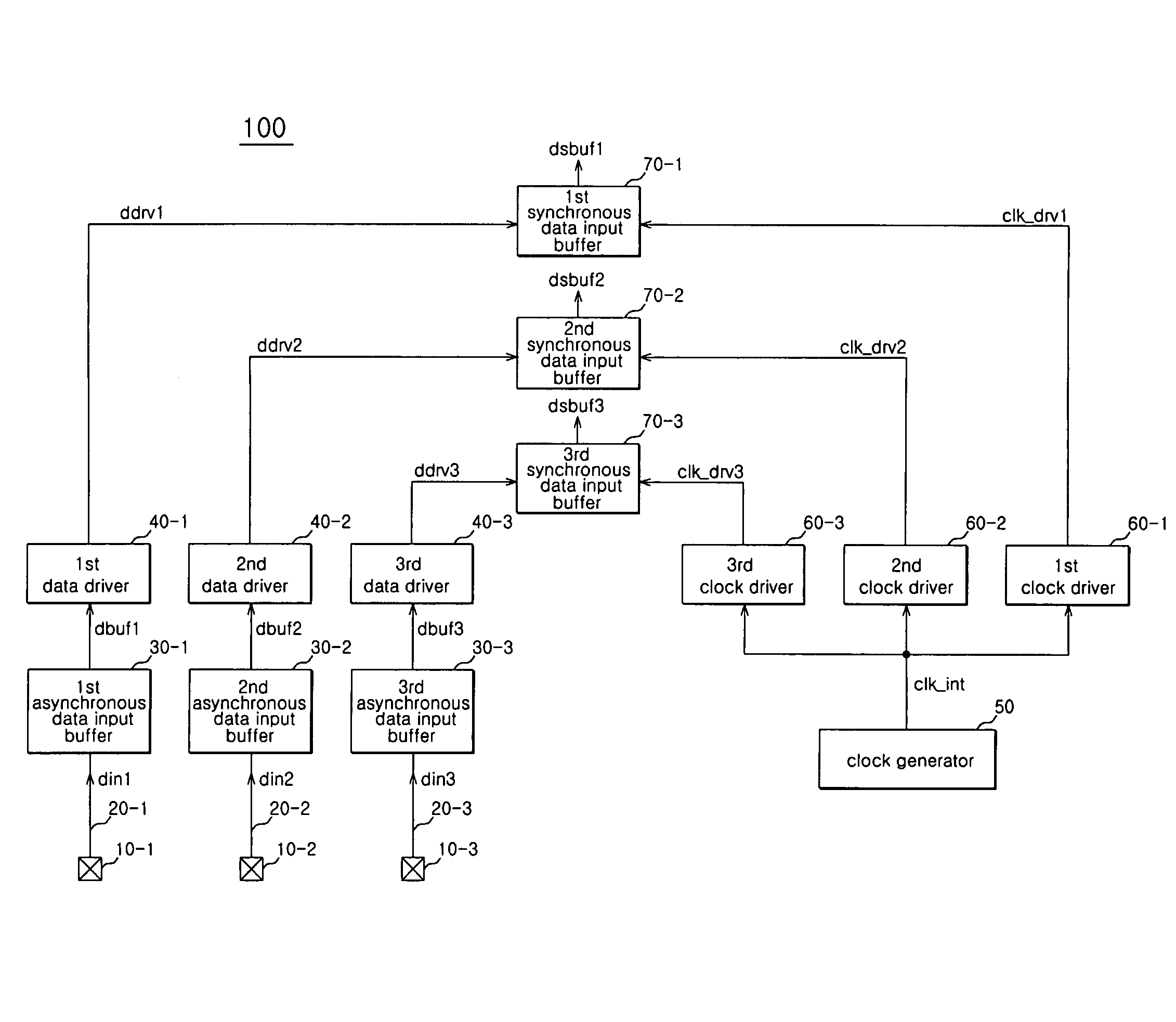
[0020]FIG. 2 is a schematic diagram of an exemplary semiconductor memory apparatus 100 according to one embodiment. In FIG. 2, for the sake of brevity a structure for performing buffering operations on data input through only 3 data pads is shown. Accordingly, more or less than 3 data pads can be provided according to the exemplary semiconductor memory apparatus.

[0021]In FIG. 2, the semiconductor memory apparatus 100 can be configured to include first to third data pads 10-1 to 10-3, first to third data lines 20-1 to 20-3, first to third asynchronous data input buffers 30-1 to 30-3, first to third data drivers 40-1 to 40-3, a clock generator 50, first to third clock drivers 60-1 to 60-3, and first to third synchronous data input buffers 70-1 to 70-3. Although not specifically shown, the semiconductor memory apparatus 100 can be integrated on a substrate. For example, one a printed circuit board / substrate, or integrated in and / or on a semiconductor substrate.

[0022]The first to third ...


PUM


Abstract

A semiconductor memory apparatus includes a clock generator configured to generate an internal clock signal, an asynchronous data input buffer configured to buffer a data input signal through a data pad to output a buffered data signal, and a synchronous data input buffer configured to buffer the buffered data signal synchronously with the internal clock signal, wherein a length of a line, through which the internal clock signal is transmitted to the synchronous data input buffer, is configured to be substantially the same with a length of a line, through which the buffered data is transmitted to the synchronous data input buffer.

Description

CROSS-REFERENCES TO RELATED APPLICATION[0001]The present application claims the benefit under 35 U.S.C 119(a) to Korean Application No. 10-2008-0086751, filed on Sep. 3, 2008, in the Korean Intellectual Property Office, which is incorporated herein by reference in its entirety as if set forth in full.BACKGROUND[0002]1. Technical Field[0003]The embodiments described herein relate to a semiconductor memory apparatus, and more particularly, to a data input circuit of a semiconductor memory apparatus.[0004]2. Related Art[0005]In general, in order to perform a data input operation, a semiconductor memory apparatus commonly includes a plurality of data pads and a plurality of data input buffers connected to respective ones of the plurality of data pads. Accordingly, respective ones of the plurality of data input buffers perform a buffering operation on data synchronously with an internal clock transmitted from a Delay Locked Loop (DLL) circuit or a Phase Locked Loop (PLL) circuit. In orde...

Claims


Application Information

Patent Timeline
Patent Type & Authority Patents(United States)
IPC IPC(8): G11C8/00
CPCG11C5/063G11C7/02G11C7/1078G11C7/1084G11C7/1093G11C29/02G11C29/022G11C29/023G11C29/028G11C7/10G11C7/22G11C8/00
Inventor LEE, JI-WANGKIM, YONG-JUHAN, SUNG-WOOSONG, HEE-WOONGOH, IC-SUKIM, HYUNG-SOOHWANG, TAE-JINCHOI, HAE-RANGJANG, JAE-MINPARK, CHANG-KUN
Owner SK HYNIX INC
Features
  • R&D
  • Intellectual Property
  • Life Sciences
  • Materials
  • Tech Scout
  • Unparalleled Data Quality
  • Higher Quality Content
  • 60% Fewer Hallucinations
Learn More