Chip carrier with reduced interference signal sensitivity
a chip carrier and interference signal technology, applied in the association of printed circuit non-printed electric components, printed capacitor incorporation, electrical apparatus construction details, etc., can solve the problems of affecting the function and reliability of the system, the miniaturization of said passive components has not been able to keep up with development, and the miniaturization of integrated circuits
- Summary
- Abstract
- Description
- Claims
- Application Information
AI Technical Summary
Benefits of technology
Problems solved by technology
Method used
Image

Examples
first embodiment
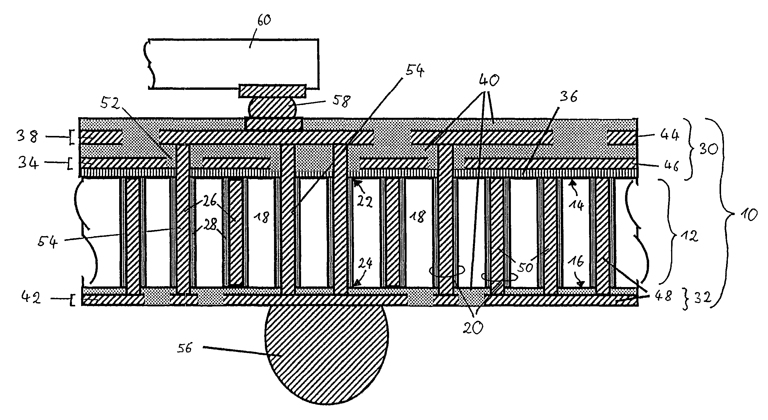
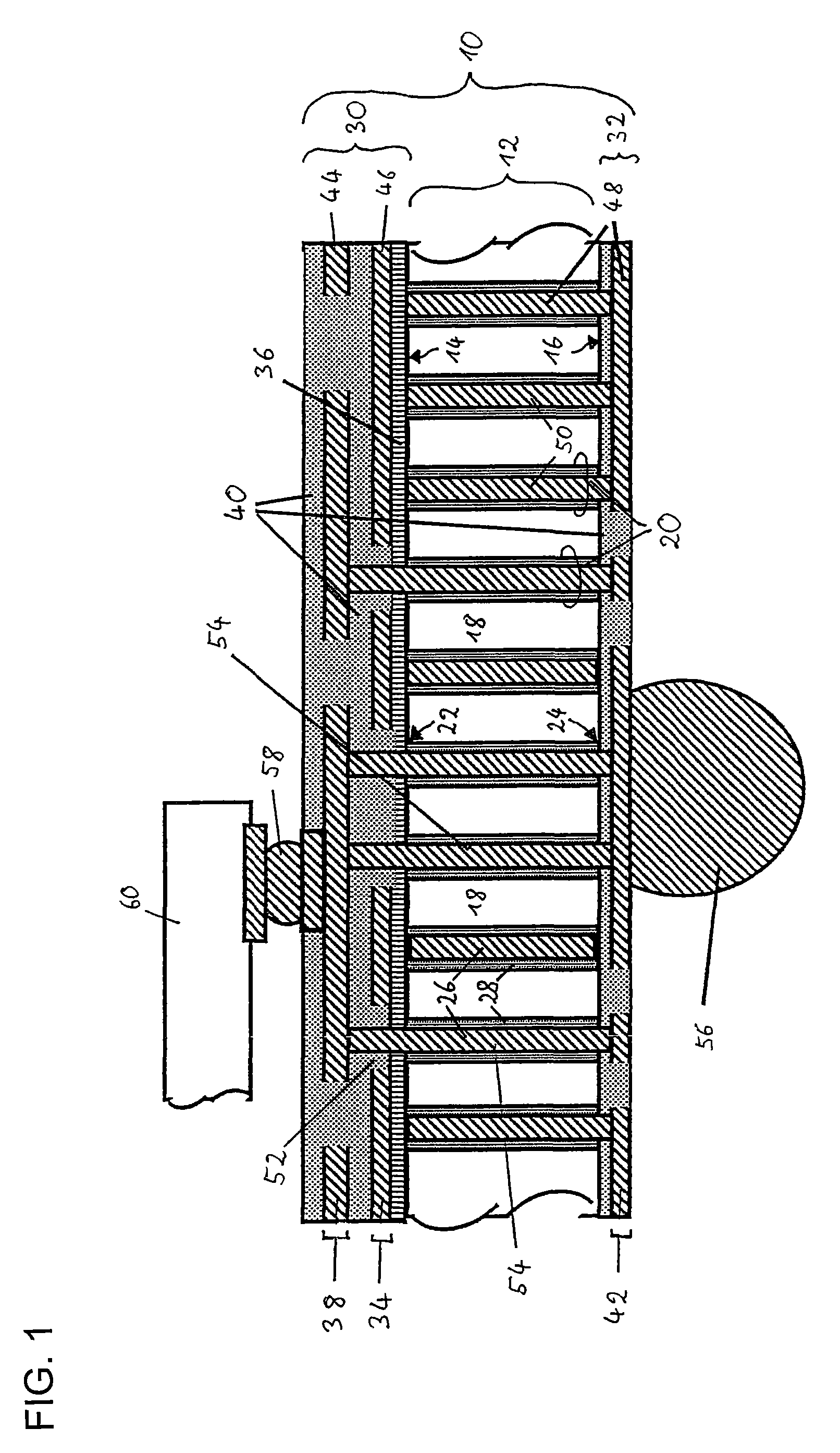
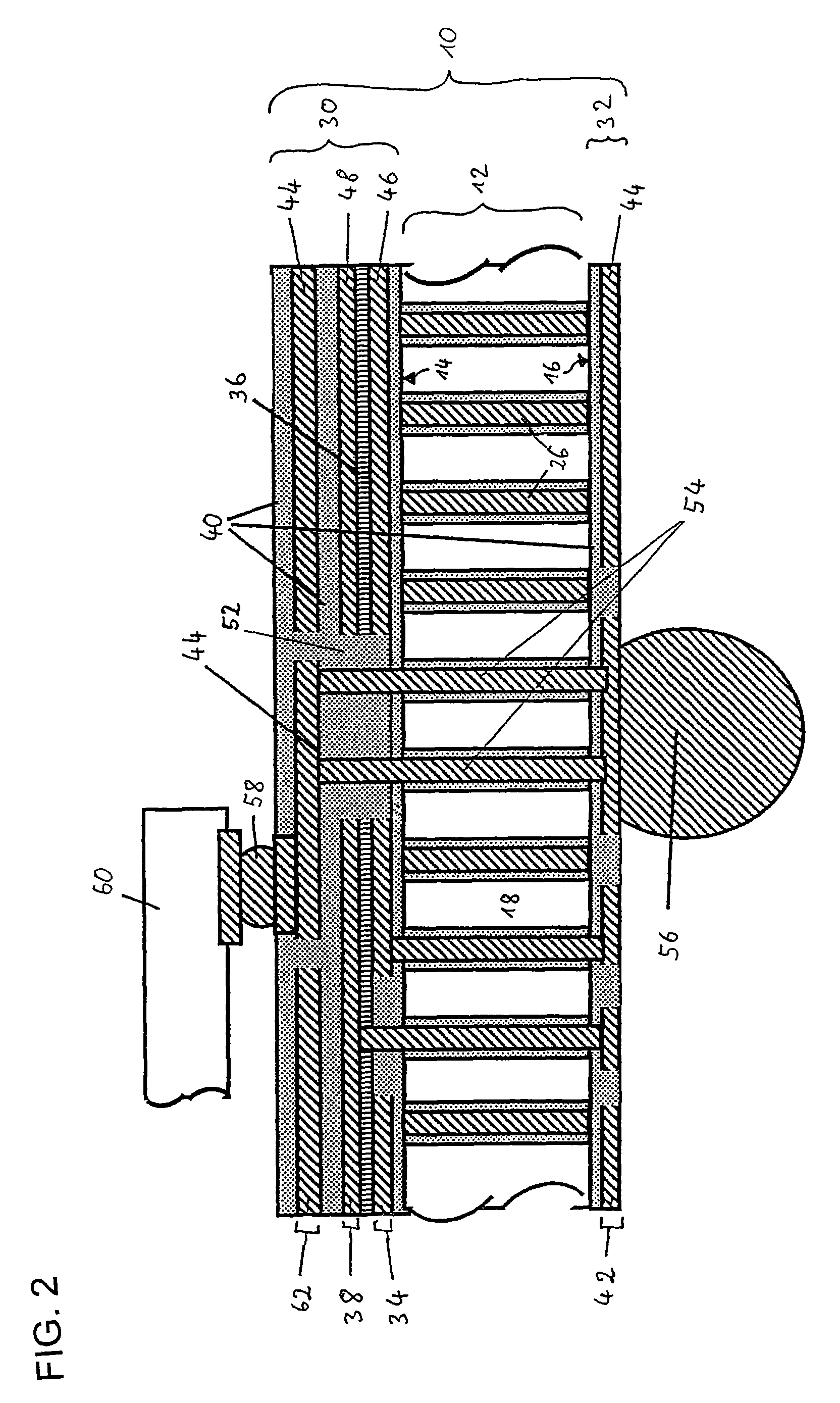
[0049]What is essential to the preferred embodiment shown is that at least one metallization layer at least partly comprises a first capacitor electrode 46 and another metallization layer at least partly comprises a second capacitor electrode 48. In the first embodiment shown, the first capacitor electrode 46 is formed at least as part of the first front-side metallization layer 34, while the second capacitor electrode 48 is at least partly comprised by the first rear-side metallization layer 42. In this embodiment, the second capacitor electrode 48 additionally comprises a plurality of capacitor fingers 50. The plurality of capacitor fingers 50 of the second capacitor electrode 48 are formed by a portion of the plated-through holes or contact channels 26 and are electrically conductively connected to that part of the second capacitor electrode 48 which is formed in the first rear-side metallization layer 42. The capacitor fingers 50 of the second capacitor electrode 48 adjoin the c...
fourth embodiment
[0073]As a result of connecting the capacitor electrodes to the poles of the supply voltage, an interference suppression of the supply system is thus effected. In this case, the arrangement of the capacitor electrode which is shown in the fourth embodiment can be understood as a series circuit of two capacitor structures. In this case, the first capacitor structure is formed between the first capacitor electrode 46 and the electrically conductively doped substrate body 18, while the transition between the substrate body 18 and the second capacitor electrode 48 forms the second capacitor structure. By means of this series circuit of the capacitances and in particular also by means of a suitable doping of the substrate body 18, it is possible to improve the quality factor of the capacitance between the capacitor electrodes, which leads to a better controllable interference suppression of the supply system.
third embodiment
[0074]In this design variant, the capacitance that can be obtained is reduced in comparison with the third embodiment shown, but the quality factors can be increased. Capacitances of approximately 500 to 1400 pF / mm2 are achieved depending on the diameter of the capacitor fingers.
[0075]A capacitor dielectric 36 having a high relative permittivity is particularly preferred. In particular, the relative permittivity of the capacitor dielectric 36 is preferably greater than the dielectric constant of the wiring insulation 40. By way of example, SiO2 could be used for the wiring insulation 40, while TiO2 and / or Al2O3 and / or Ta2O5 and / or HfO2 and / or Si3N4 and / or ONO (in particular the layer structure SiO2 / Si3N4 / SiO2) is particularly well suited as the capacitor dielectric 36. In particular in the first, third and fourth embodiments, the passage insulation 28 also preferably has a high relative permittivity. The production of this dielectric layer with a high capacitance may be effected e.g...
PUM
 Abstract
Description
Claims
Application Information
 - R&D
- Intellectual Property
- Life Sciences
- Materials
- Tech Scout
- Unparalleled Data Quality
- Higher Quality Content
- 60% Fewer Hallucinations
Browse by: Latest US Patents, China's latest patents, Technical Efficacy Thesaurus, Application Domain, Technology Topic, Popular Technical Reports.
© 2025 PatSnap. All rights reserved.Legal|Privacy policy|Modern Slavery Act Transparency Statement|Sitemap|About US| Contact US: help@patsnap.com