Gate driving method and circuit for liquid crystal display

a technology driving methods, which is applied in the direction of electric digital data processing, instruments, computing, etc., can solve the problems of affecting the performance affecting the flicker effect of large-scale lcds, and affecting the performance of large-scale lcds, so as to achieve the effect of substantially improving the flicker effect and increasing the charging time of liquid crystal capacitors

Active Publication Date: 2011-04-12
AU OPTRONICS CORP
View PDF20 Cites 22 Cited by
  • Summary
  • Abstract
  • Description
  • Claims
  • Application Information

AI Technical Summary

Benefits of technology

[0019]Accordingly, the present invention is directed to a driving method and a driving circuit of a liquid crystal display which can minimize the difference of the feed-through voltages at the front portion and the end portion of the same scan line to reduce the flicker effect during display.
[0020]The present invention is also directed to a driving method and a circuit of a liquid crystal display which can increase the charging time of the liquid crystal capacitor.
[0029]According to the methods and structures of the present invention, a negative voltage square wave signal is used for correction before the gate driving signal with the positive voltage square wave is applied to the scan line. The corrected gate driving signal is then applied to the scan line. Because the negative voltage square signal is also affected by the stray capacitance and the stray resistance of the scan line, the difference of the high voltage level and the low voltage level at the declining edge of the gate driving signal on the same whole scan line will be substantially equal. As a result, the feed-through voltages are also equal. Not only can the flicker effect be substantially improved, but the charging time of the liquid crystal capacitor is also increased.

Problems solved by technology

Large-size LCDs, however, have a serious issue.
The larger the screens of LCDs, the more serious the flicker on the screens of LCDs.
During the LCD semiconductor manufacturing process, stray capacitance and resistance are generated on the scan line, which causes RC delay and eventually results in the distortion of the waveform. FIG. 3A is a configuration showing a control signal waveform outputted from a gate driver IC of the LCD.
The situation becomes worse when the screen size of the LCD is increased.
In addition, the larger the screen size of the LCD, the longer the scan line, and the worse the RC delay.
Therefore, the charging time is insufficient.
For manufacturing a large-size LCD with high resolution, the insufficient charging time would work against it.
Another issue when driving the LCD is the feed-through effect.
The voltage difference would result in a flicker effect.
This method, however, cannot prevent the waveform distortion effect caused by the RC delay on the scan line.
The flicker effect still cannot be resolved.

Method used


Image

  • Gate driving method and circuit for liquid crystal display
  • Gate driving method and circuit for liquid crystal display
  • Gate driving method and circuit for liquid crystal display

Examples


Embodiment Construction

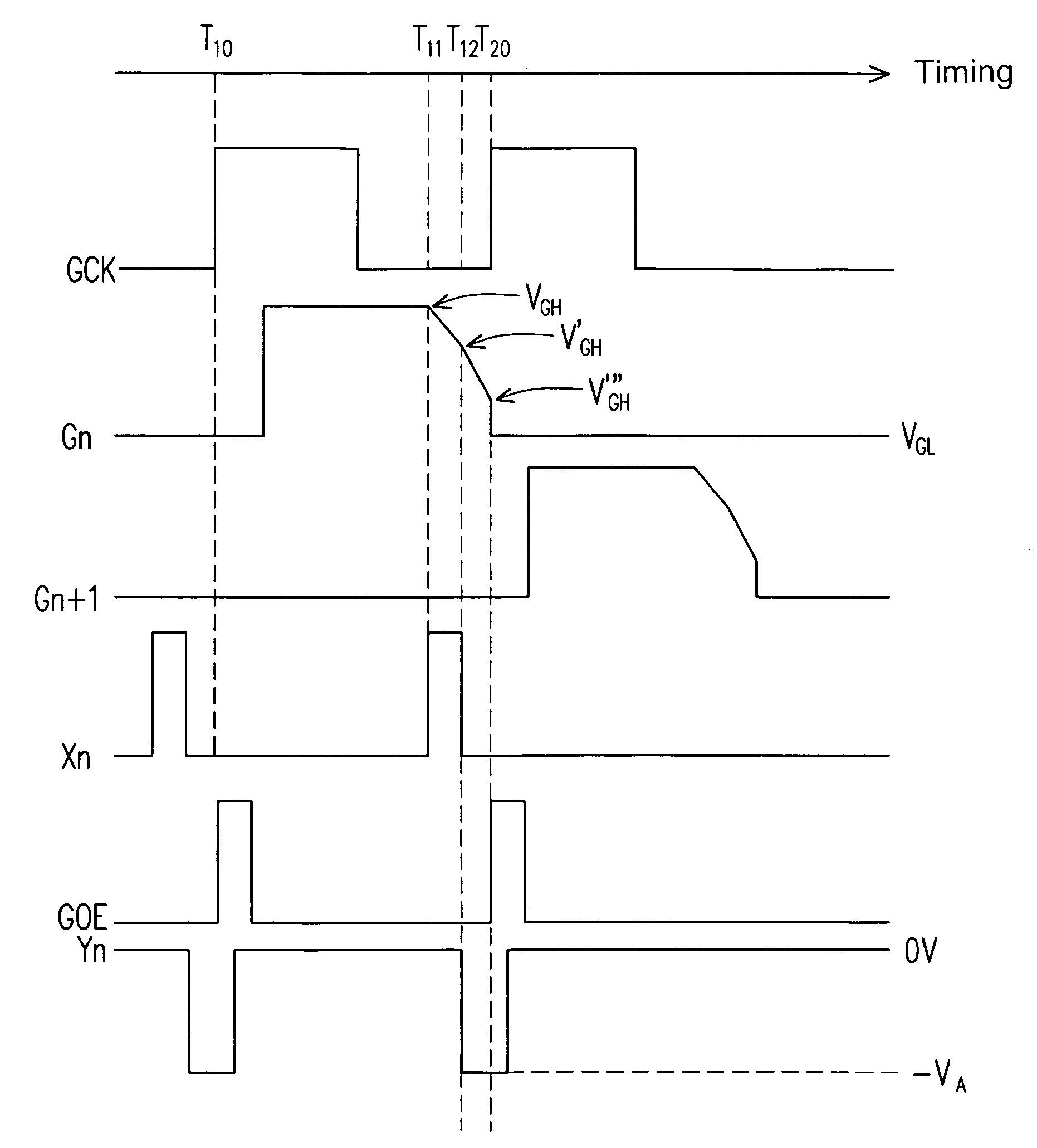
[0044]The technical feature of the present invention is to minimize difference of feed-through voltage of transistors on the same scan line so as to reduce the flicker effect during display. In the present invention, it is assumed that CGD / (CGD+CLC+Cst) in the formula (1) is a constant. The voltage difference at the end of the driving signal is modified by merely adjusting ΔV.

[0045]Since the inputted positive voltage square wave signal, i.e., the gate driving signal, would trigger the described issues in the conventional technology, the inputted negative voltage square wave signal would also be affected by the stray capacitance and resistance of the scan line when passing through. Accordingly, if a negative voltage square wave signal, i.e., a correction signal, is superposed to the positive voltage square wave signal to generate a corrected gate driving signal, the difference of voltage drops of the positive voltage square wave signal at the front and the end portions of the scan li...


PUM


Abstract

A gate driving method for a liquid crystal display (LCD) and a gate driver thereof are provided. The LCD has a plurality of scan lines. The method starts by generating a gate driving signal. A correction signal is superposed to the gate driving signal to generate a corrected gate driving signal and to reduce a high voltage level of the gate driving signal, wherein a polarity of the correction signal is opposite to a polarity of the gate driving signal. The corrected gate driving signal is then outputted to drive one of the corresponding scan lines.

Description

CROSS-REFERENCE TO RELATED APPLICATION[0001]This application claims the priority benefit of Taiwan application serial no. 93132699, filed on Oct. 28, 2004. All disclosure of the Taiwan application is incorporated herein by reference.BACKGROUND OF THE INVENTION[0002]1. Field of the Invention[0003]The present invention relates to an improved method for driving a liquid crystal display, and more particularly to a method of reducing flickers and a method of increasing charging time of a liquid crystal display.[0004]2. Description of the Related Art[0005]Liquid crystal displays (LCDs) have become popular in recent years. Not only can LCDs save spaces, but power consumption can also be reduced. LCDs with large sizes and high resolutions have replaced traditional displays, such as cathode radiation tube displays. Large-size LCDs, however, have a serious issue. The larger the screens of LCDs, the more serious the flicker on the screens of LCDs.[0006]FIG. 1 is a configuration showing a basic...

Claims


Application Information

Patent Timeline
Patent Type & Authority Patents(United States)
IPC IPC(8): G09G3/36
CPCG09G3/3648G09G2310/06G09G2320/0247G09G2320/0223G09G2320/0219
Inventor HSU, WEN-FAYI, CHIEN-YU
Owner AU OPTRONICS CORP
Why Eureka
Try Eureka