Supercharge Your Innovation With Domain-Expert AI Agents!

Array substrate for a liquid crystal display device and method of manufacturing the same

a liquid crystal display device and array substrate technology, applied in non-linear optics, instruments, optics, etc., can solve problems such as deteriorating the electric characteristic of thin film transistors, and achieve the effect of reducing the influence of parasitic capacitors and reducing ligh

Inactive Publication Date: 2011-07-26
LG DISPLAY CO LTD
View PDF3 Cites 0 Cited by
  • Summary
  • Abstract
  • Description
  • Claims
  • Application Information

AI Technical Summary

Benefits of technology

[0016]An advantage of the present invention is to provide an array substrate for a liquid crystal display device and a manufacturing method thereof that reduces the influence of the parasitic capacitor at the crossing area of the gate and data lines.
[0017]Another advantage of the present invention is to provide an array substrate for a liquid crystal display device and a manufacturing method thereof that reduces the influence of light from the backlight device.

Problems solved by technology

The transmitted and reflected light can reach the active layer of the thin film transistor T, thus deteriorating the electric characteristic of the thin film transistor.

Method used


Image

  • Array substrate for a liquid crystal display device and method of manufacturing the same
  • Array substrate for a liquid crystal display device and method of manufacturing the same
  • Array substrate for a liquid crystal display device and method of manufacturing the same

Examples


Embodiment Construction

[0030]Reference will now be made in detail to embodiment of the present invention, which are illustrated in the accompanying drawings.

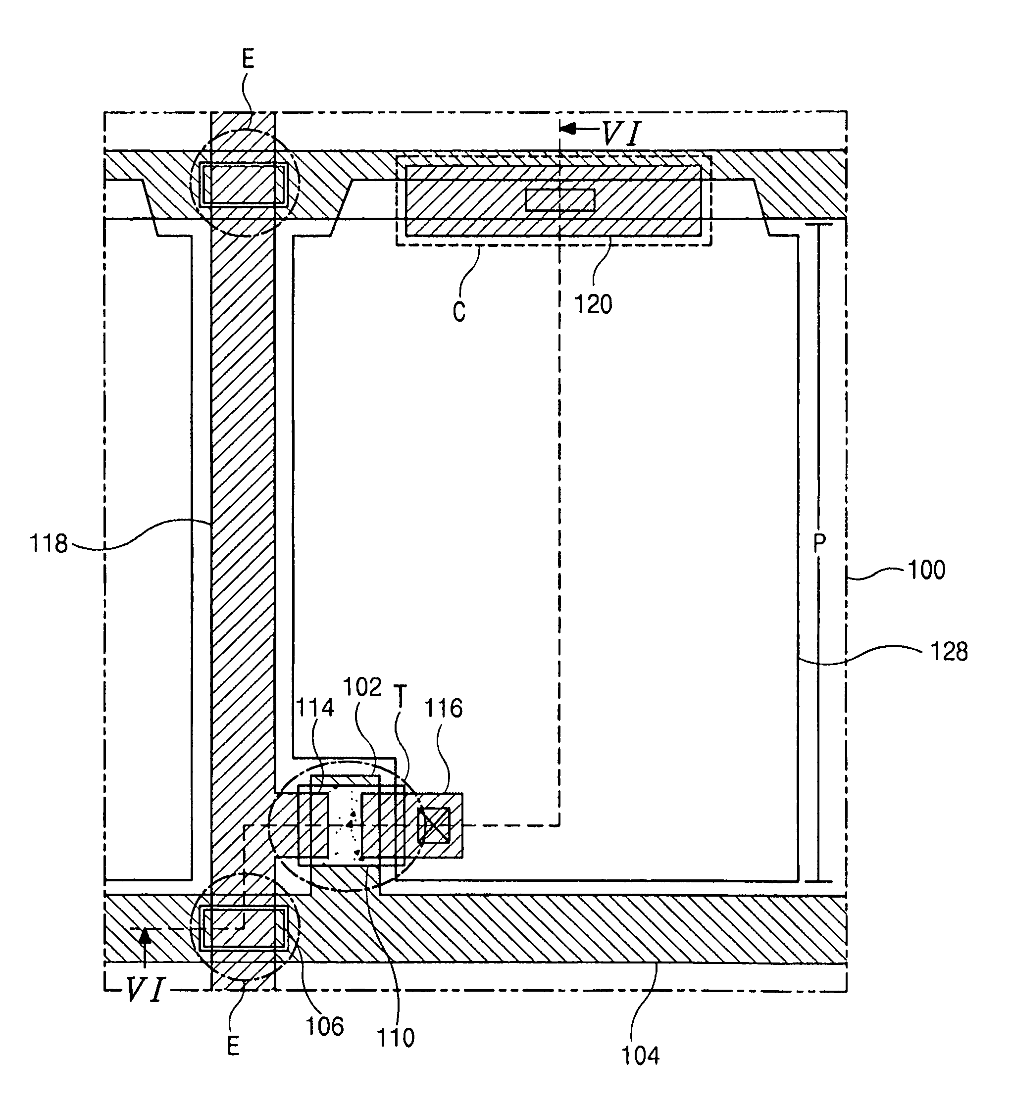
[0031]FIG. 5 is a similar view to FIG. 4. Gate lines 104 and data lines 118 are formed on a substrate 100 to cross each other, thereby defining pixel areas P.

[0032]A thin film transistor T is formed at the crossing of each of the gate and data lines 104 and 118 to function as a switching element. The thin film transistor T includes a gate electrode 102 that is connected to the gate line 104 to receive scanning signals, a source electrode 114 that is connected to the data line 118 and receives data signals, and a drain electrode 116 that is spaced apart from the source electrode 114. In addition, the thin film transistor T includes an active layer 110 between the gate electrode 102 and the source and drain electrodes 114 and 116, and a transparent pixel electrode 128 which is formed in the pixel area P and is connected to the drain electrode 116. The p...


PUM

PropertyMeasurementUnit
voltageaaaaaaaaaa
electric fieldaaaaaaaaaa
liquidaaaaaaaaaa

Abstract

An array substrate for a liquid crystal display device includes a substrate, a gate line elongated in one direction, a data line crossing over the gate line, a thin film transistor near a crossing point of the gate and data lines and connected to the gate and data lines, an independent portion under the data line at the crossing point, the portion being separated from the gate line, and a pixel electrode connected to the thin film transistor. The independent portion may be inside the gate line. The parasitic capacitor between the gate line and the data line can be reduced and the amount of light from the backlight device can be reduced.

Description

[0001]This application is a divisional application of application Ser. No. 10 / 736,571 filed Dec. 17, 2003 now U.S. Pat. No. 7,349,038 which claims the benefit of Korean Patent Application No. 10-2002-0082730 filed Dec. 23, 2002 which are hereby incorporated by reference for all purposes as if fully set forth herein.BACKGROUND OF THE INVENTION[0002]1. Field of the Invention[0003]The present invention relates to an array substrate for a liquid crystal display (LCD) device and more particularly, to an array substrate having gate and data lines and a manufacturing method thereof.[0004]2. Discussion of the Related Art[0005]Generally, a liquid crystal display (LCD) device includes two substrates that are spaced apart and face each other with a liquid crystal material layer interposed between the two substrates. Each of the substrates includes electrodes that face each other, wherein a voltage applied to each electrode induces an electric field between the electrodes and within the liquid ...

Claims


Application Information

Patent Timeline
Patent Type & Authority Patents(United States)
IPC IPC(8): G02F1/136G02F1/1362
CPCG02F1/136286G02F1/136
Inventor PARK, DAE-LIMHWANG, SEONG-SOOKIM, YOUNG-SIKMOON, SOO-HWAN
Owner LG DISPLAY CO LTD
Features
  • R&D
  • Intellectual Property
  • Life Sciences
  • Materials
  • Tech Scout
  • Unparalleled Data Quality
  • Higher Quality Content
  • 60% Fewer Hallucinations
Learn More