Supercharge Your Innovation With Domain-Expert AI Agents!

Surface emitting laser array

a laser array and surface technology, applied in the direction of lasers, semiconductor lasers, laser details, etc., can solve the problems of increasing the number of process steps, crystal defects on the disconnected surface, and resonances that may interfere with each other, and achieve high-density arrays easily

Inactive Publication Date: 2011-08-02
CANON KK
View PDF23 Cites 1 Cited by
  • Summary
  • Abstract
  • Description
  • Claims
  • Application Information

AI Technical Summary

Benefits of technology

Enables high-density arraying of surface emitting lasers without degrading their characteristics, reduces optical crosstalk, and simplifies electrical wiring by maintaining continuous active layers and eliminating the need for reflector structures.

Problems solved by technology

More specifically, in the case where the laser oscillation wavelengths are the same between those surface emitting lasers, resonators may interfere with each other.
In the case of disconnecting the active layer between the surface emitting lasers adjacent to each other for this reason, such a disconnection becomes an obstacle for integrated high-density arraying, and a crystal defect may occur from the disconnected surfaces.
This may also lead to the increase in the number of process steps.
Further, when the active layer is disconnected, if the disconnected width between the surface emitting lasers adjacent to each other is small, it is difficult to stop the guiding of light to another surface emitting laser.
However, the application of the configuration of Japanese Patent Application Laid-Open No. 2003-273456 leads to the following problem.
That is, for arraying laser elements, a reflector structure is provided between the surface emitting lasers adjacent to each other, but the provision of such a reflector structure hinders high-density arraying.
In particular, when the reflector structure 450 is provided, it is difficult to suppress the transmission of light from a laser element to another laser element without disconnecting the active layer that is a waveguide.
Further, the disconnection of the active layer causes the above-mentioned problems.
However, if the reflector structure as described above is provided, compared with the case where there is no reflector structure between elements and the surface of the slab layer 320 is flat, it is more difficult to install electric wiring necessary in the case of electrically driving each laser element of the surface emitting laser array.
Thus, also in this respect, high-density arraying may be become difficult.

Method used


Image

  • Surface emitting laser array
  • Surface emitting laser array
  • Surface emitting laser array

Examples


example 1

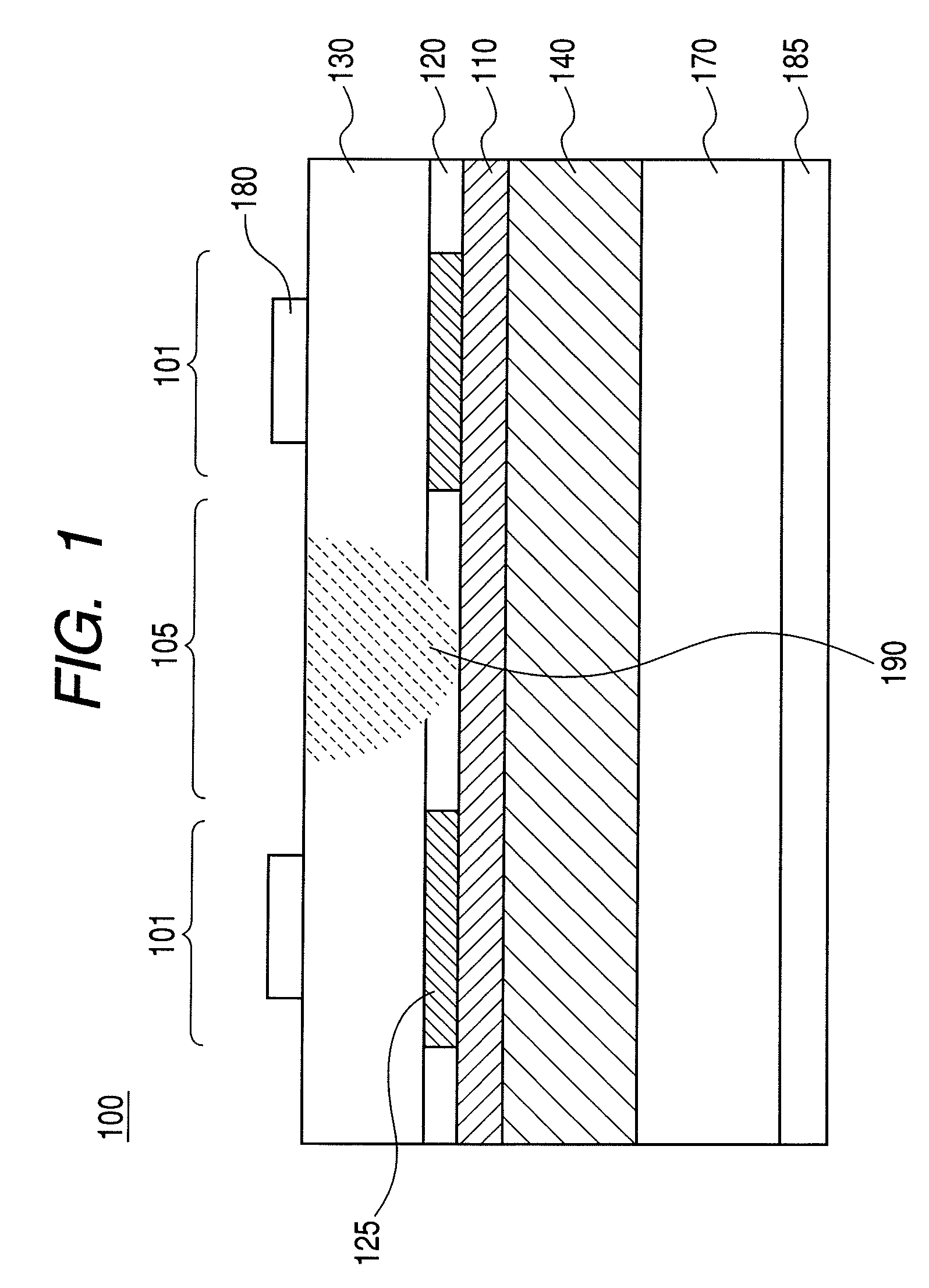
[0093]In Example 1, a surface emitting laser array to which the present invention is applied is described. FIG. 1 is a schematic cross-sectional view illustrating a surface emitting laser array of the present example. In FIG. 1, a surface emitting laser array 100 includes a substrate 170, a multilayer mirror 140, an active layer and spacer layer 110, a slab layer 120, a cladding layer 130, an upper electrode 180, and a lower electrode 185. A photonic crystal 125 is formed in the slab layer 120.

[0094]A region 190 is electrically insulated.

[0095]According to the present example, in the surface emitting laser array 100, multiple surface emitting lasers 101 are provided with a non-laser region 105 interposed therebetween.

[0096]A substrate and the multilayer mirror are, for example, n-doped and a slab layer and a cladding layer are, for example, p-doped with the active layer interposed therebetween.

[0097]When a voltage is applied between the upper electrode 180 provided for each of the s...

example 2

[0126]In Example 2, an exemplary configuration of a surface emitting laser array to which the present invention is applied is described, in which each laser is driven by optical excitation as a unit for driving the surface emitting laser array.

[0127]FIG. 9 is a schematic cross-sectional view for describing an exemplary configuration of the surface emitting laser array of the present example.

[0128]In FIG. 9, a surface emitting laser array 1000 includes a surface emitting laser 1001, an excitation source 1095, and excited light 1096.

[0129]In the surface emitting laser array 1000 in Example 2, the multilayer mirror 140, the active layer 110, and the slab layer 120 are formed on the substrate 170 in the same way as in Example 1. The photonic crystal 125 is formed on the slab layer 120.

[0130]The cladding layer 130 is formed on the slab layer. The cladding layer 130 may be air. The surface emitting laser array 1000 includes the excitation source 1095 capable of causing optical excitation ...

example 3

[0132]In Example 3, an exemplary configuration in which light absorber is provided between the respective surface emitting lasers of the surface emitting laser array of Example 1 is described.

[0133]FIG. 10 is a schematic cross-sectional view illustrating the surface emitting laser array in the present example.

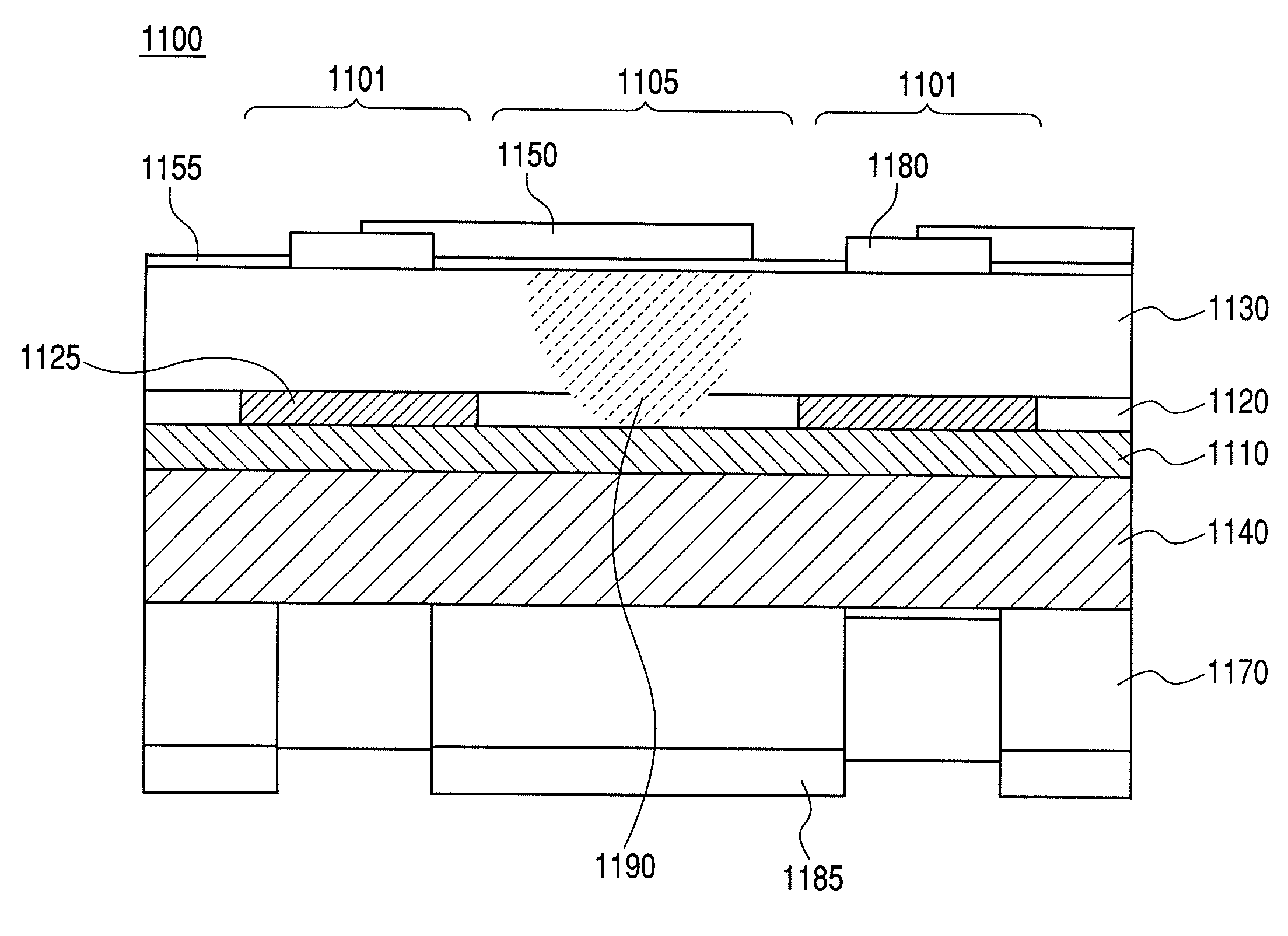
[0134]In FIG. 10, a surface emitting laser array 1100 includes a surface emitting laser 1101, a region 1105 between the respective surface emitting lasers, an active layer 1110, a slab layer 1120, photonic crystal structures 1125, a cladding layer 1130, and a multilayer mirror 1140. The surface emitting laser array 1100 further includes a light absorber 1150 that is an absorber of laser resonant light, a passivation film 1155, a substrate 1170, an upper electrode 1180, a lower electrode 1185, and an electrically insulated region 1190.

[0135]In the same way as in Example 1, the multilayer mirror 1140, the active layer 1110, the slab layer 1120, and the cladding layer 1130 are for...


PUM


Abstract

Provided is a surface emitting laser array using a photonic crystal, which allows an active layer to be shared without disconnecting the active layer between the individual surface emitting lasers adjacent to each other, and enables high-density arraying easily. The surface emitting laser array includes: at least two surface emitting lasers formed on a substrate, each having a laminated structure of multiple semiconductor layers including a semiconductor multilayer mirror, an active layer, and a photonic crystal having a refractive index profile in an in-plane direction, the photonic crystal and the semiconductor multilayer mirror in the laminated structure forming a waveguide for guiding light in a resonance mode; and a region without the photonic crystal provided between adjacent surface emitting lasers in the surface emitting laser array, in which the surface emitting lasers have the same semiconductor multilayer mirror and the same active layer.

Description

TECHNICAL FIELD[0001]The present invention relates to a surface emitting laser array using a photonic crystal. For example, the present invention relates to a surface emitting laser array that can also be used as a light source for conducting drawing on a photosensitive drum of an image forming apparatus such as a copying machine or a laser printer.BACKGROUND ART[0002]Recently, a surface emitting laser for emitting laser light perpendicularly to a substrate has been studied extensively because the surface emitting laser can be advantageously arrayed two-dimensionally, compared with an edge emitting laser.[0003]Further, recently, a surface emitting laser using a photonic crystal has been studied.[0004]As such a surface emitting laser using a photonic crystal, Japanese Patent Application Laid-Open No. 2000-332351 describes a configuration in which an active layer is sandwiched between cladding layers having a refractive index lower than that of the active layer and a photonic crystal ...

Claims


Application Information

Patent Timeline
Patent Type & Authority Patents(United States)
IPC IPC(8): H01S5/00
CPCB82Y20/00H01S5/42H01S5/041H01S5/105H01S5/2027H01S5/2063H01S5/2081H01S5/34326H01S5/34333H01S2301/176H01S5/11
Inventor IKUTA, MITSUHIRO
Owner CANON KK
Features
  • R&D
  • Intellectual Property
  • Life Sciences
  • Materials
  • Tech Scout
  • Unparalleled Data Quality
  • Higher Quality Content
  • 60% Fewer Hallucinations
Learn More