Supercharge Your Innovation With Domain-Expert AI Agents!

Semiconductor mask inspection using die-to-die and die-to-database comparisons

a semiconductor and mask technology, applied in the field of mask forming method and semiconductor device manufacturing method, can solve the problems of reducing the degree of pattern forming faithfulness in ensuring inspection, increasing workload, and fine graphics not always reflected faithfully on the actual pattern (mask pattern) actually formed

Active Publication Date: 2011-10-11
KIOXIA CORP
View PDF14 Cites 2 Cited by
  • Summary
  • Abstract
  • Description
  • Claims
  • Application Information

AI Technical Summary

Benefits of technology

This approach reduces the number of false defects detected, allowing for more accurate inspection and maintaining inspection throughput, thereby reducing the need for manual classification and equipment time, enabling the inspection of entire masks without storage limitations.

Problems solved by technology

However, fine graphics are not always reflected faithfully on a pattern (mask pattern) actually formed on a mask.
Thus, there has been established a situation in which the lowered degree of pattern forming faithfulness cannot be ignored in guaranteeing an inspection result.
For example, in a mask defect inspection of Die-to-Database comparison method (Jpn. Pat. Appln. KOKAI Publication No. 2002-23345), the following problem occurs due to the lowered degree of pattern forming faithfulness.
In this classifying work, a workload increases due to a trend for downsizing semiconductor devices.
However, the automated classifying work is still poor in reliability.
Therefore, there has not been established a situation in which a classifying work by visual inspection can be eliminated.
Under such a situation as described above, a tremendous number of false defects occur in one mask due to the downsizing of a pattern and due to the downsizing of an OPC correction grid (correction unit).
Specifically, false defects may occur in number exceeding an upper limit of defects in number that can be maintained (stored) in a defect inspection apparatus.
In this case, there has been established a situation in which the whole mask cannot be inspected.
However, in general, a pattern forming region of one mask is not formed of only the same pattern group, and all the defects in a desired region of the mask cannot always be detected by only the defect inspection of the Die-to-Die comparison method.

Method used


Image

  • Semiconductor mask inspection using die-to-die and die-to-database comparisons
  • Semiconductor mask inspection using die-to-die and die-to-database comparisons
  • Semiconductor mask inspection using die-to-die and die-to-database comparisons

Examples


Embodiment Construction

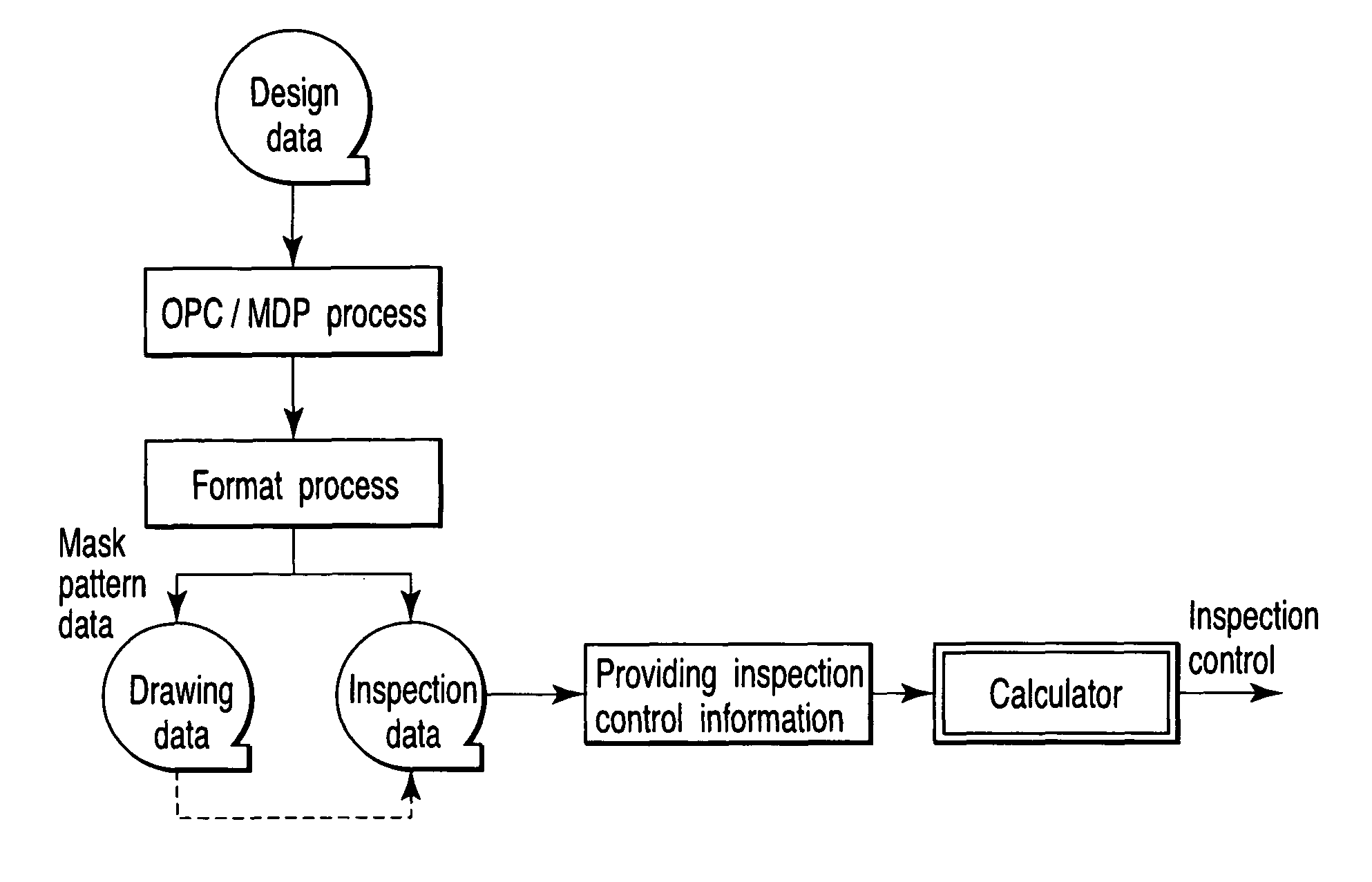
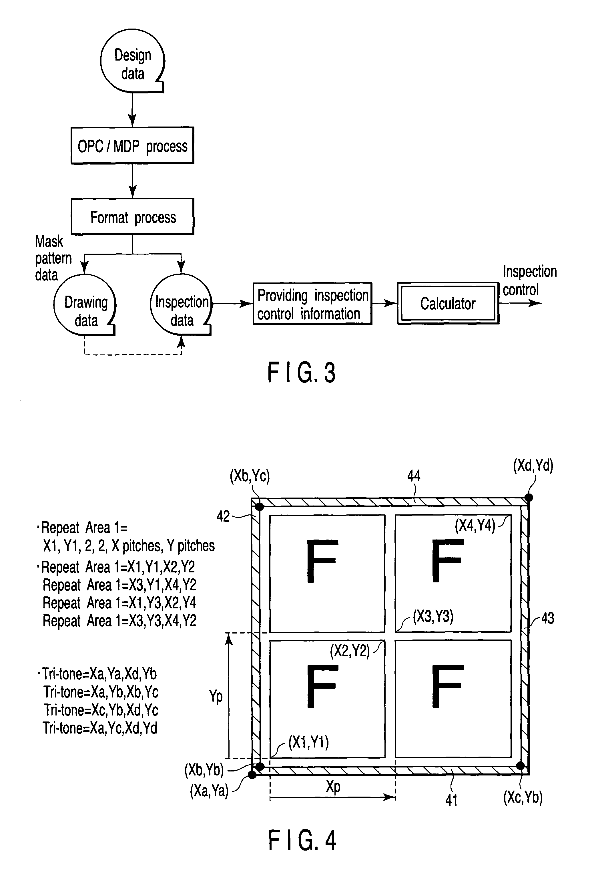
[0025]Embodiments of the present invention will be described hereinafter with reference to the drawings.

[0026]FIG. 1 is a block diagram depicting a schematic configuration of a mask defect inspection apparatus used in an embodiment of the present invention.

[0027]In the figure, reference numeral 11 designates an XY table. On the XY table, a mask 12 used in manufacturing a semiconductor device is placed. The XY table 11 is driven in an X direction (horizontal direction on the plane) and in a Y direction (vertical direction on the plane) a stage control circuit 14 having received a command from a calculator 13.

[0028]A position of the XY stage 11 is monitored by a laser interferometer (not shown). Positional information of the monitored XY stage 11 is inputted to the stage control circuit 14. The stage control circuit 14 controls the XY stage 11 having the mask 12 placed thereon with high precision on the basis of the inputted positional information.

[0029]On the other hand, a light sour...


PUM

PropertyMeasurementUnit
defect inspectionaaaaaaaaaa
transparentaaaaaaaaaa
optical proximity effect correctionaaaaaaaaaa

Abstract

A mask forming method includes preparing design data of mask including pattern regions having identical repetition patterns respectively, generating mask pattern data of mask based on the design data, generating inspection control information for controlling inspection of defect on mask based on the mask pattern data, the information including positional information of the pattern regions and inspection sensitivity information of the repetition pattern, providing the inspection control information to mask pattern data, forming mask pattern of mask based on the mask pattern data, and inspecting the mask pattern based on the mask pattern data comprising inspecting portion in the mask pattern different from the pattern regions by Die-to-Database comparison method, the inspecting the portion including selecting portion corresponding to repetition pattern from the mask pattern based on the positional information, and inspecting the selected portion by Die-to-Die comparison method at an inspection sensitivity corresponding to inspection sensitivity information.

Description

CROSS-REFERENCE TO RELATED APPLICATIONS[0001]This application is based upon and claims the benefit of priority from prior Japanese Patent Application No. 2005-152435, filed May 25, 2005, the entire contents of which are incorporated herein by reference.BACKGROUND OF THE INVENTION[0002]1. Field of the Invention[0003]The present invention relates to a mask forming method and a semiconductor device manufacturing method used in lithography process of semiconductor process.[0004]2. Description of the Related Art[0005]In recent years, the downsizing of semiconductor devices has been in progress. As a result, in a mask manufacturing process, a correction process for correcting an optical proximity effect (OPC: Optical Proximity Correction) has been carried out. By the OPC process, fine graphics such as fine pattern steps or fine pattern irregularities are formed on design data.[0006]Mask pattern data at the time of forming a mask pattern (data obtained by applying a required process such a...

Claims


Application Information

Patent Timeline
Patent Type & Authority Patents(United States)
IPC IPC(8): G06K9/00G03F1/84
CPCG03F1/84
Inventor IKENAGA, OSAMUTSUTSUI, TOMOHIRO
Owner KIOXIA CORP
Features
  • R&D
  • Intellectual Property
  • Life Sciences
  • Materials
  • Tech Scout
  • Unparalleled Data Quality
  • Higher Quality Content
  • 60% Fewer Hallucinations
Learn More