Supercharge Your Innovation With Domain-Expert AI Agents!

One-step synthesis and patterning of aligned polymer nanowires on a substrate

a polymer nanowire and substrate technology, applied in the field of polymer nanostructures, can solve the problems of inapplicability of the above approaches, and the inability to achieve simple and scalable techniques for producing high-quality and controllable polymer nanowire arrays

Inactive Publication Date: 2011-11-08
GEORGIA TECH RES CORP
View PDF2 Cites 5 Cited by
  • Summary
  • Abstract
  • Description
  • Claims
  • Application Information

AI Technical Summary

Benefits of technology

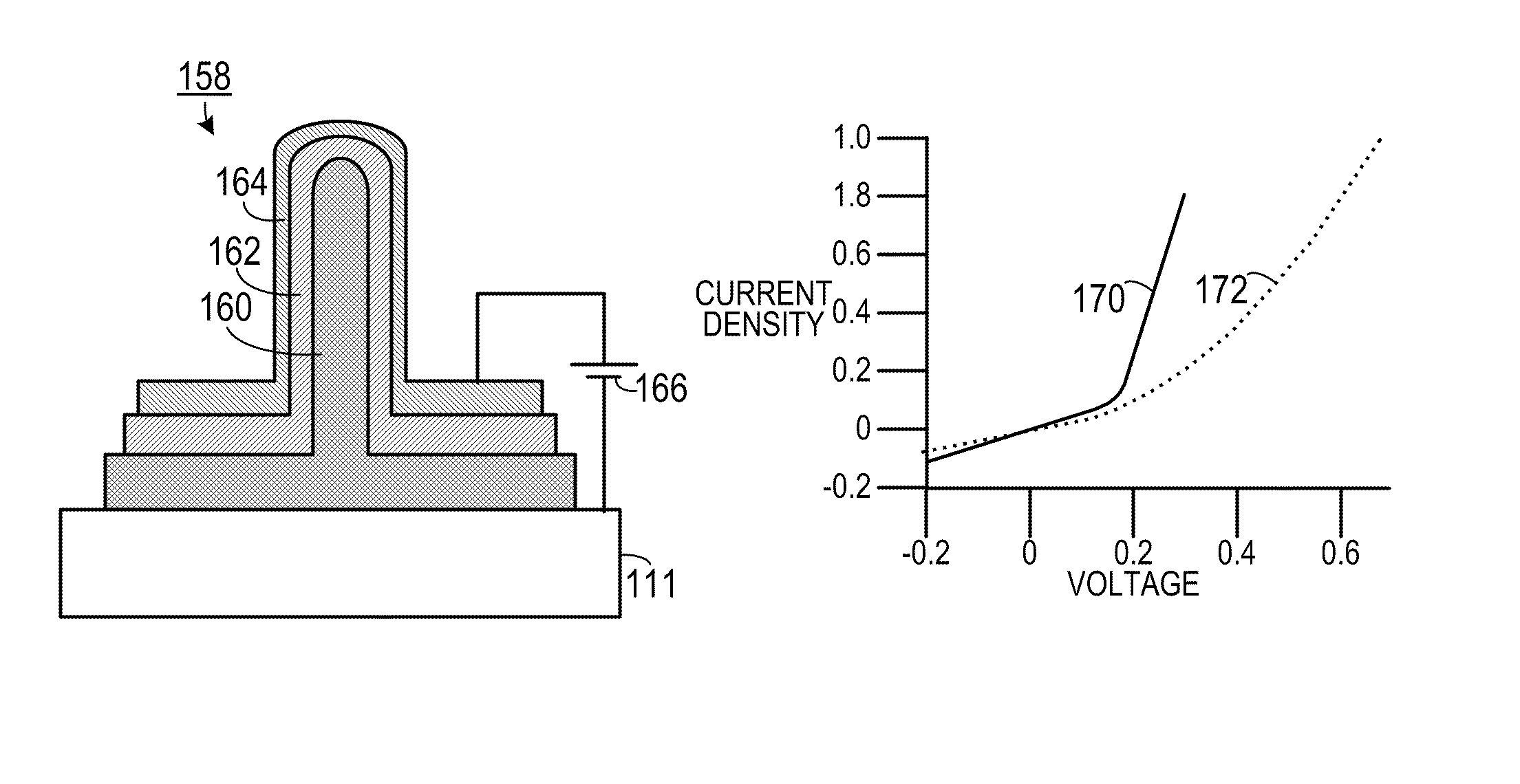
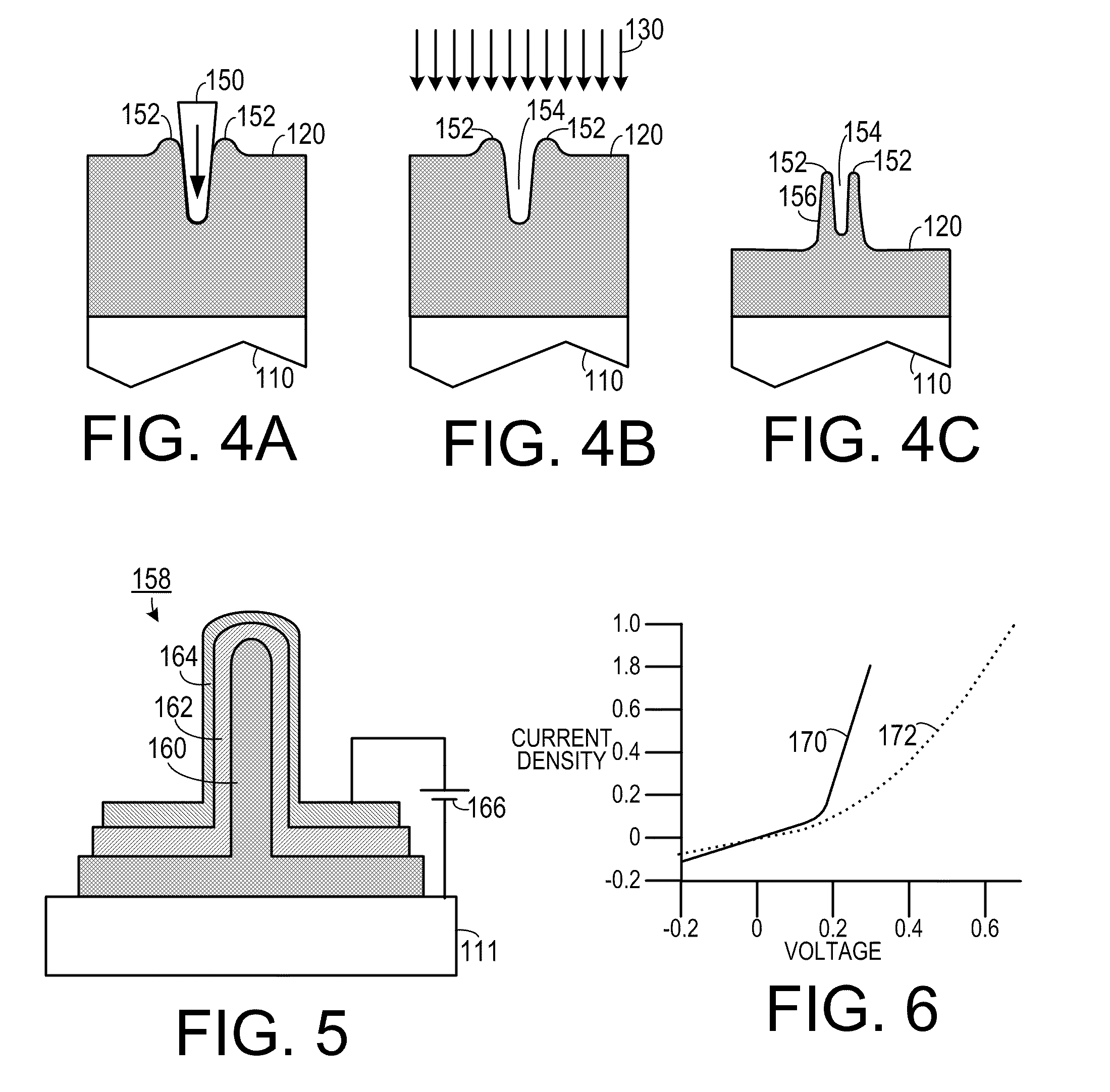
This method enables the production of high-performance polymer nanowire arrays with enhanced charge transport properties, suitable for flexible electronics, OLEDs, and biosensors, demonstrating improved current density and light emission compared to conventional thin film devices.

Problems solved by technology

There is an emerging need to fabricate high-performance polymer nanowire (PNW) based nanodevices for flexible electronics and photonics, but the above approaches are likely inapplicable for such purpose.
Although templating, chemical synthesis, and even a few ion generating techniques have yielded some such devices, they do not lend themselves to simple and scalable techniques for producing high quality and controllable polymer nanowire arrays with the ability to pattern these polymer nanowires over a large scale.

Method used


Image

  • One-step synthesis and patterning of aligned polymer nanowires on a substrate
  • One-step synthesis and patterning of aligned polymer nanowires on a substrate
  • One-step synthesis and patterning of aligned polymer nanowires on a substrate

Examples


Embodiment Construction

A preferred embodiment of the invention is now described in detail. Referring to the drawings, like numbers indicate like parts throughout the views. Unless otherwise specifically indicated in the disclosure that follows, the drawings are not necessarily drawn to scale. As used in the description herein and throughout the claims, the following terms take the meanings explicitly associated herein, unless the context clearly dictates otherwise: the meaning of “a,”“an,” and “the” includes plural reference, the meaning of “in” includes “in” and “on.”“Nanostructure” means a structure having at least one dimension that is less than 1 micrometer.

Also, as used herein “ITO” means indium tin oxide; “MEH-PPV” means poly[2-methoxy-5-(2′-ethyl-hexyloxy)-1,4-phenylene vinylene; “PEDOT:PSS” means (poly(3,4-ethylenedioxythiophene)poly(styrenesulfonate); means “PVDF” (polyvinylidene difluoride); “PPY” means polymer polypyrrole; “SU8” means an epoxy-based photoresist; and “PMMA” means poly(methyl met...


PUM

PropertyMeasurementUnit
temperatureaaaaaaaaaa
diametersaaaaaaaaaa
diametersaaaaaaaaaa

Abstract

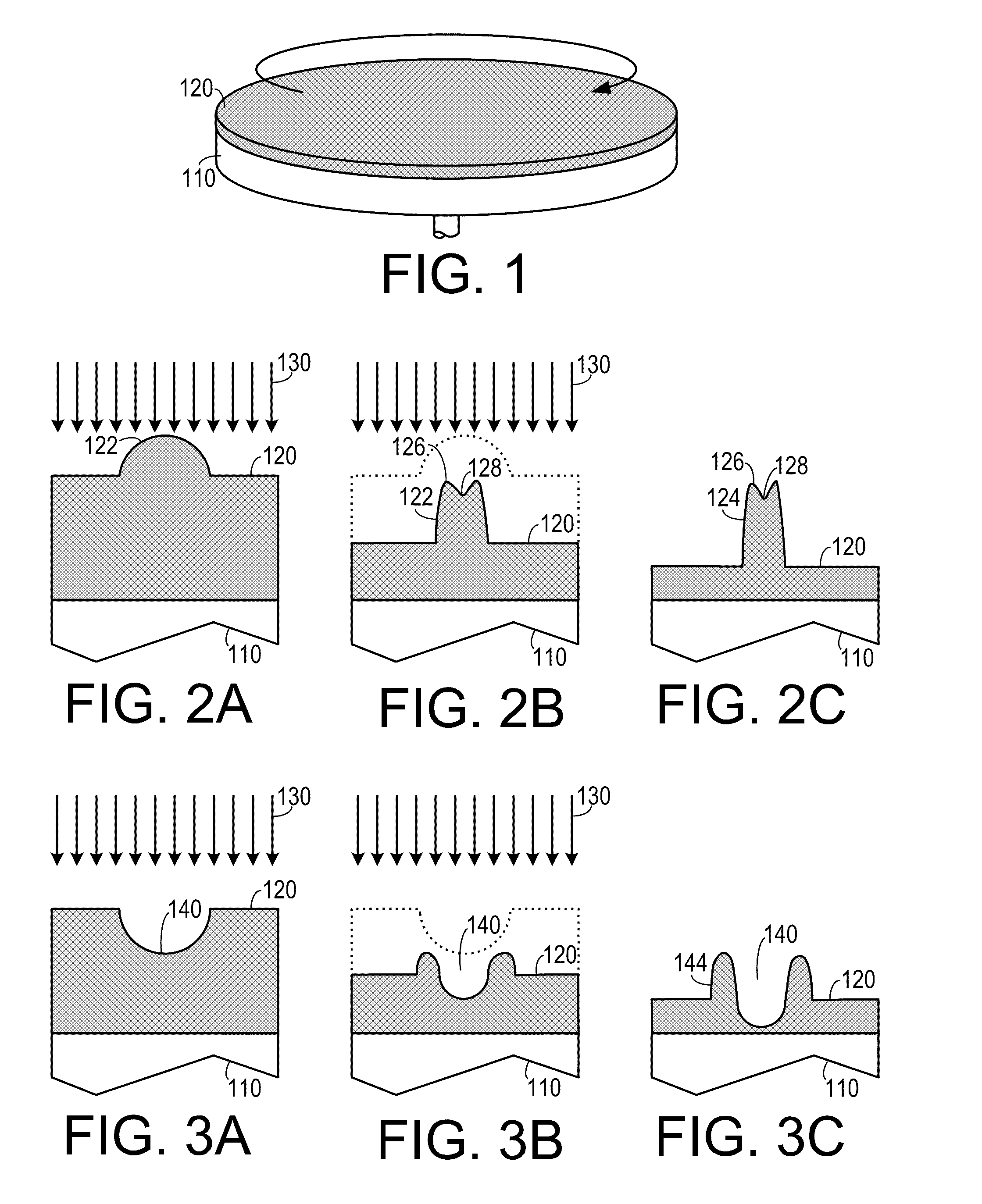
In a method of making a polymer structure on a substrate a layer of a first polymer, having a horizontal top surface, is applied to a surface of the substrate. An area of the top surface of the polymer is manipulated to create an uneven feature that is plasma etched to remove a first portion from the layer of the first polymer thereby leaving the polymer structure extending therefrom. A light emitting structure includes a conductive substrate from which an elongated nanostructure of a first polymer extends. A second polymer coating is disposed about the nanostructure and includes a second polymer, which includes a material such that a band gap exists between the second polymer coating and the elongated nanostructure. A conductive material coats the second polymer coating. The light emitting structure emits light when a voltage is applied between the conductive substrate and the conductive coating.

Description

BACKGROUND OF THE INVENTION1. Field of the InventionThe present invention relates to polymer nanostructures and, more specifically, to a method of synthesizing aligned polymer nanostructures.2. Description of the Prior ArtAligned nanowires of inorganic semiconductor materials have important applications in photonics, electronics, sensing, bioscience and energy science. Highly desirable in such applications is cost-effective growth of high quality, patterned and uniformly aligned nanowires on a large scale. Aligned inorganic nanowire arrays can be grown using either the vapor-liquid-solid and vapor-solid-solid process at high temperature (>˜500° C.) with the assistance of catalyst particles, or the seed assisted chemical growth at low temperature.There is an emerging need to fabricate high-performance polymer nanowire (PNW) based nanodevices for flexible electronics and photonics, but the above approaches are likely inapplicable for such purpose. Although templating, chemical synt...

Claims


Application Information

Patent Timeline
Patent Type & Authority Patents(United States)
IPC IPC(8): H01L21/31H01L21/469
CPCB82Y20/00B82Y30/00H01L51/0014H01L51/0017H01L51/0037H01L51/0038H01L51/52H01L51/56H01L2251/5338H10K71/20H10K71/231H10K85/1135H10K85/114H10K50/80H10K2102/311H10K71/00
Inventor WANG, ZHONG L.WANG, XUDONGMORBER, JENNY R.LIU, JIN
Owner GEORGIA TECH RES CORP
Features
  • R&D
  • Intellectual Property
  • Life Sciences
  • Materials
  • Tech Scout
  • Unparalleled Data Quality
  • Higher Quality Content
  • 60% Fewer Hallucinations
Learn More