Supercharge Your Innovation With Domain-Expert AI Agents!

Light emitter substrate and image displaying apparatus using the same

a technology of light emitter substrate and image displaying apparatus, which is applied in the direction of discharge tube luminescnet screen, discharge tube with electrostatic control, etc., and can solve the problems of device destruction, increased potential difference between adjacent metal backs, and deterioration of withstanding discharge structur

Inactive Publication Date: 2011-12-06
CANON KK
View PDF34 Cites 0 Cited by
  • Summary
  • Abstract
  • Description
  • Claims
  • Application Information

AI Technical Summary

Benefits of technology

[0009]The present invention aims to improve, in a light emitter substrate which has a resistor for connecting electrodes adjacent in a row direction, withstand discharge performance of the resistor. Moreover, the present invention aims to provide an image displaying apparatus which uses the light emitter substrate like this.
[0012]According to the present invention, in the light emitter substrate which has the resistor for connecting the electrodes adjacent in the row direction, it is possible to improve the withstand discharge performance of the resistor. Moreover, according to the present invention, it is possible to provide the image displaying apparatus which uses the light emitter substrate like this.

Problems solved by technology

However, if a discharge occurs in a case where further high voltage is applied to improve luminance, a potential difference between the adjacent metal backs increases, whereby there is a possibility that a secondary discharge occurs between the adjacent metal backs.
Besides, if the resistor is arranged between the adjacent metal backs, discharge voltage of a material of the resistor is lower than surface discharge voltage between the metal backs according to a kind of the relevant material, whereby there is a possibility that withstand discharge structure is destroyed.
If the secondary discharge occurs, the discharging current increases, whereby there is a possibility that a damage such as device destruction or the like which is not preferable for image displaying occurs.

Method used


Image

  • Light emitter substrate and image displaying apparatus using the same
  • Light emitter substrate and image displaying apparatus using the same
  • Light emitter substrate and image displaying apparatus using the same

Examples


example 1

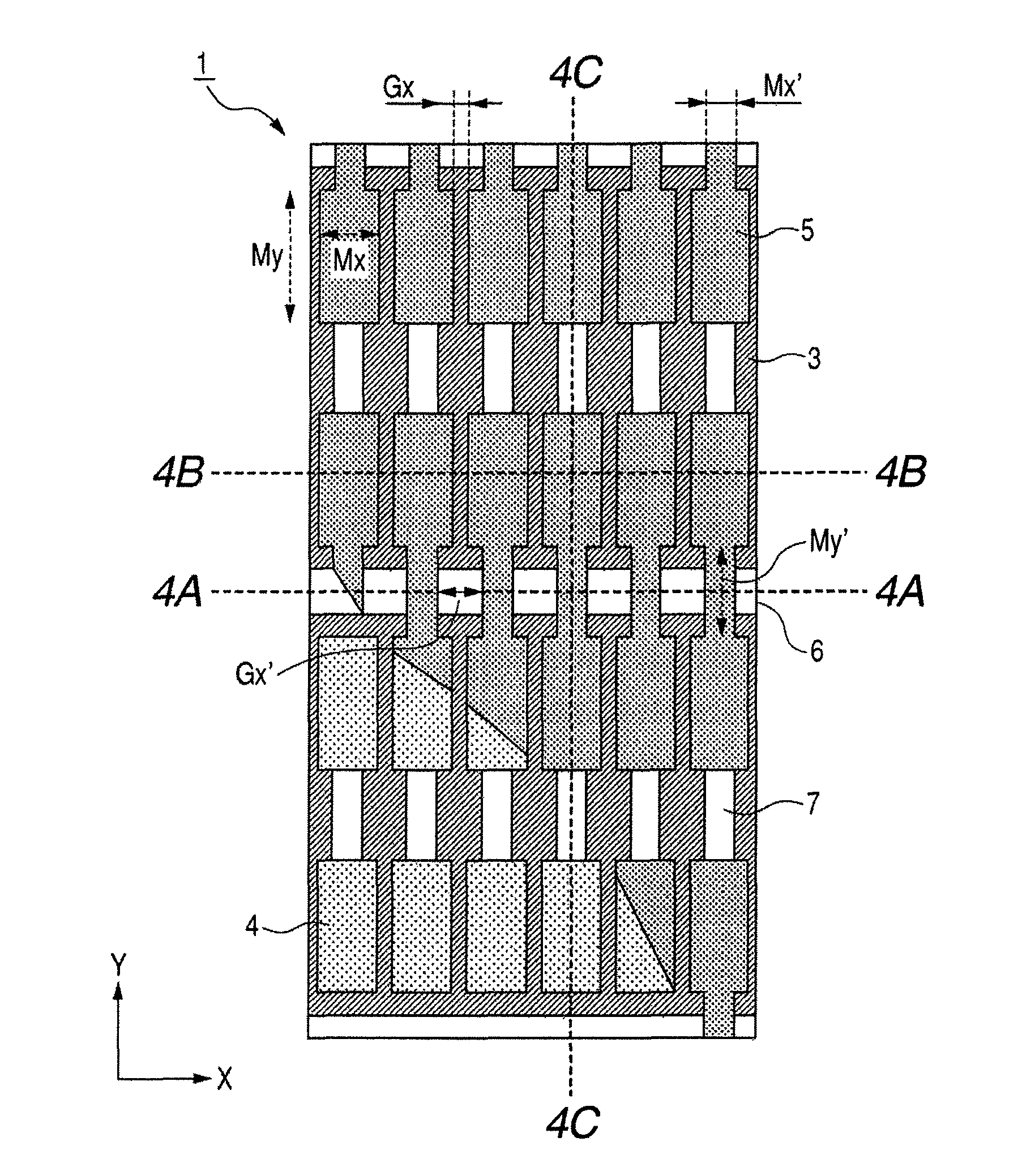
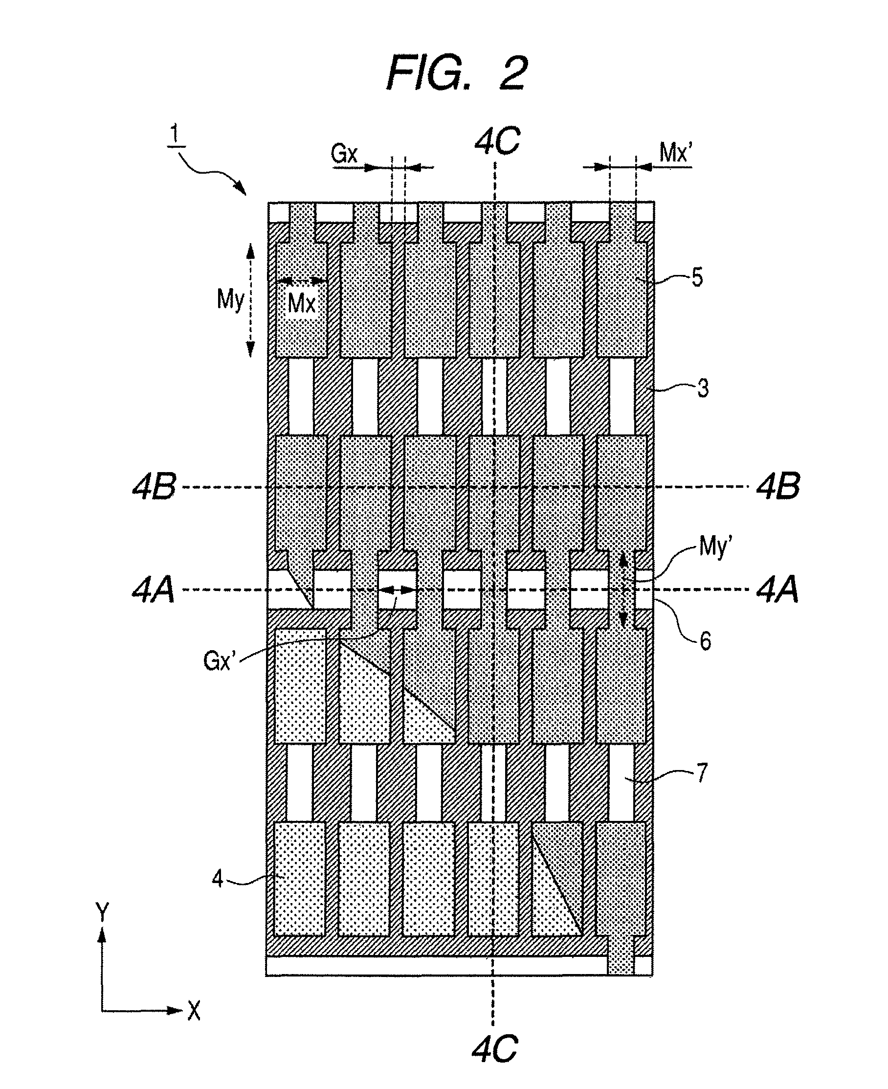
[0036]This example is an example of a light emitter substrate illustrated in FIGS. 2, 3, 4A, 4B and 4C. FIG. 2 is an inner face view, where a metal back of the light emitter substrate is partially cut off. The light emitter substrate of this example was manufactured as described below.

[0037]A lattice-like shape, which has apertures only on desired regions in a light emitting region, is screen printed on a surface of a cleaned glass substrate by using a black paste (NP-7803D available by Noritake Co., Ltd.), and the glass substrate is baked at the temperature 550° C. after drying it at the temperature 120° C. to form a black member 3 of which thickness is 5 μm. Pitches of aperture portions were set to become 450 μm in the Y direction and 150 μm in the X direction, which are same as those in device pitches on a rear plate, and the size of an aperture portion is set to become 220 μm in the Y direction and 90 μm in the X direction.

[0038]A high-resistance paste, in which a ruthenium oxid...

example 2

[0044]This example is different from Example 1 in a point that the metal back 5 is formed to cover the three light-emitting members 4 adjacent to each other in the column direction (Y direction) as illustrated in FIG. 5. The row-direction resistors 6 are arranged corresponding to narrow width portions of the metal backs. In addition, the column-direction resistors 7 are arranged on the rows where the row-direction resistors 6 are not arranged, that is, arranged every three rows.

[0045]As to a light emitter substrate 16 manufactured in this manner, although the resistance design is same as that in Example 1, the volume resistance of a resistant paste can be doubled, and the discharge voltage of the row-direction resistors 6 and the column-direction resistors 7 can be increased.

[0046]An SED is manufactured by using this light emitter substrate 16, and when a discharge inducing experiment similar to that in Example 1 was conducted by applying the voltage of 10 kV between the light emitt...

example 3

[0047]This example is different from Example 1 in a point that the metal back 5 is formed to cover the six light-emitting members 4 in total consisted by two members adjacent to each other in the column direction and three members adjacent to each other in the row direction as illustrated in FIG. 6. The column-direction resistors 7 are arranged on the rows where the row-direction resistors 6 are not arranged, that is, one line is arranged every two columns. That is, one line is arranged between the metal backs adjacent to each other in the column direction (Y direction).

[0048]The row direction width (Mx) and the column direction width (My) at portions of covering the light-emitting members 4 of the metal backs 5 were respectively set to become 350 μm and 330 μm, and the row direction width (Mx′) and the column direction width (My′) on narrow width portions were respectively set to become 150 μm and 120 μm. As a result, the resistance Rx and the resistance Ry respectively became leve...


PUM


Abstract

It aims to improve, in a light emitter substrate which has a resistor for connecting electrodes adjacent in a row direction, withstand discharge performance of the resistor. In the light emitter substrate which comprises a substrate, plural light-emitting members which are positioned in matrix on the substrate, plural electrodes each of which covers at least one of the light-emitting members and which are positioned in matrix, and a row-direction resistor which is positioned between the electrodes adjacent in the row direction and connects these electrodes to each other, a row-direction separated distance Gx′ between the electrodes adjacent in the row direction at a connecting portion between the electrodes and the row-direction resistor is larger than a row-direction separated distance Gx between the electrodes adjacent in the row direction at a portion covering the light-emitting members (Gx′>Gx).

Description

BACKGROUND OF THE INVENTION[0001]1. Field of the Invention[0002]The present invention relates to a light emitter substrate and an image displaying apparatus which uses the light emitter substrate.[0003]2. Description of the Related Art[0004]Conventionally, an image displaying apparatus which comprises an electron source substrate having plural electron-emitting devices arranged in matrix and a light emitter substrate having plural light-emitting members arranged in matrix and opposed to the plural electron-emitting devices has been known. In the image displaying apparatus like this, the light emitter substrate and the electron source substrate are typically opposed to each other at a gap of about several millimeters, and high voltage of, e.g., approximately 10 kV is applied between these substrates. For these reasons, a discharge occurs easily, and, if the discharge once occurs, a discharging current flows from the whole of a metal back which has been integrally formed, whereby an i...

Claims


Application Information

Patent Timeline
Patent Type & Authority Patents(United States)
IPC IPC(8): H01J1/62H01J31/12
CPCH01J1/53H01J29/085H01J31/127H01J2329/08H01J2329/28
Inventor YAMAZAKI, KOJIDATE, TAKASHIINOUE, YUKIHIRO
Owner CANON KK
Features
  • R&D
  • Intellectual Property
  • Life Sciences
  • Materials
  • Tech Scout
  • Unparalleled Data Quality
  • Higher Quality Content
  • 60% Fewer Hallucinations
Learn More