Check patentability & draft patents in minutes with Patsnap Eureka AI!

Lead pin for package substrate

a technology of lead pins and substrates, which is applied in the direction of coupling device connections, sustainable manufacturing/processing, semiconductor/solid-state device details, etc., can solve the problems of inclination of lead pins, difficult to maintain uniform bonding strength, and high melting temperature of soldering

Inactive Publication Date: 2012-03-27
SAMSUNG ELECTRO MECHANICS CO LTD
View PDF17 Cites 4 Cited by
  • Summary
  • Abstract
  • Description
  • Claims
  • Application Information

AI Technical Summary

Benefits of technology

The design prevents solder paste bulging and void formation, maintaining the lead pin's vertical alignment and enhancing bonding strength by allowing voids to be discharged laterally, thus reducing the likelihood of defects and ensuring reliable connection.

Problems solved by technology

The T-type lead pin has gradually become widespread due to limitation of the available area for the circuit configuration of the package substrate as compared to the pin insert type.
However, the T-type lead pin has disadvantages in that the lead pin is inclined and it is difficult to maintain uniform bonding strength when being mounted on the package substrate.
In particular, as the use of lead has been recently limited in consideration of environmental effects due to the soldering, a soldering (Sn—Ag—Cu, and Sn—Sb) not using lead has been used, such that a melting temperature of the soldering becomes high.
As the melting temperature for soldering becomes high, a soldering for connecting lead pins that support lead pins is melted by reflow heat during a reflow process for mounting an IC chip on a package substrate, thereby causing inclination of the lead pins.
If any one of them is inclined, the CPU itself cannot be mounted on a socket, such that the package substrate itself is regarded as a defective product.
Further, there is a possibility that voids are formed between the head part of the lead pin and a soldering when soldering the T-type lead pin according to the related art in addition to the inclination of the lead pin.
However, in order to minimize thermal impact that is applied to the package substrate 10 during the reflow process, the heating time at the temperature of the melting point or more is controlled to be short, such that there is insufficient time to remove the voids 13 in the soldering.

Method used


Image

  • Lead pin for package substrate
  • Lead pin for package substrate
  • Lead pin for package substrate

Examples


Embodiment Construction

[0037]The acting effects and technical configuration with respect to the objects of a lead pin for a package substrate according to the present invention will be clearly understood by the following description in which exemplary embodiments of the present invention are described with reference to the accompanying drawings.

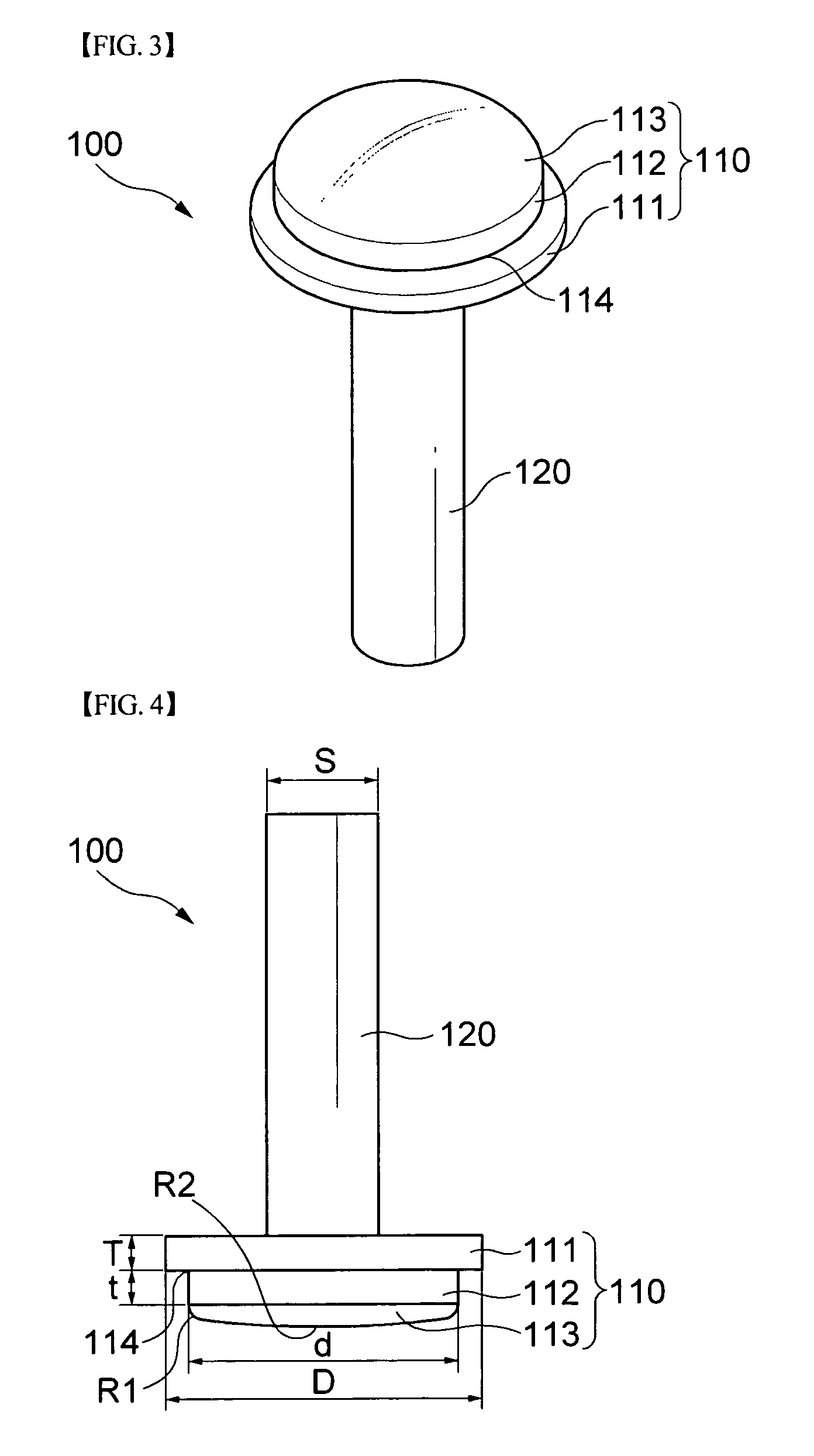
[0038]First, FIG. 3 is a bottom perspective view of a lead pin for a package substrate according to the present invention, FIG. 4 is a side view of a lead pin for a package substrate according to the present invention, and FIGS. 5 and 6 are a plan view and a bottom view of a lead pin for a package substrate according to the present invention.

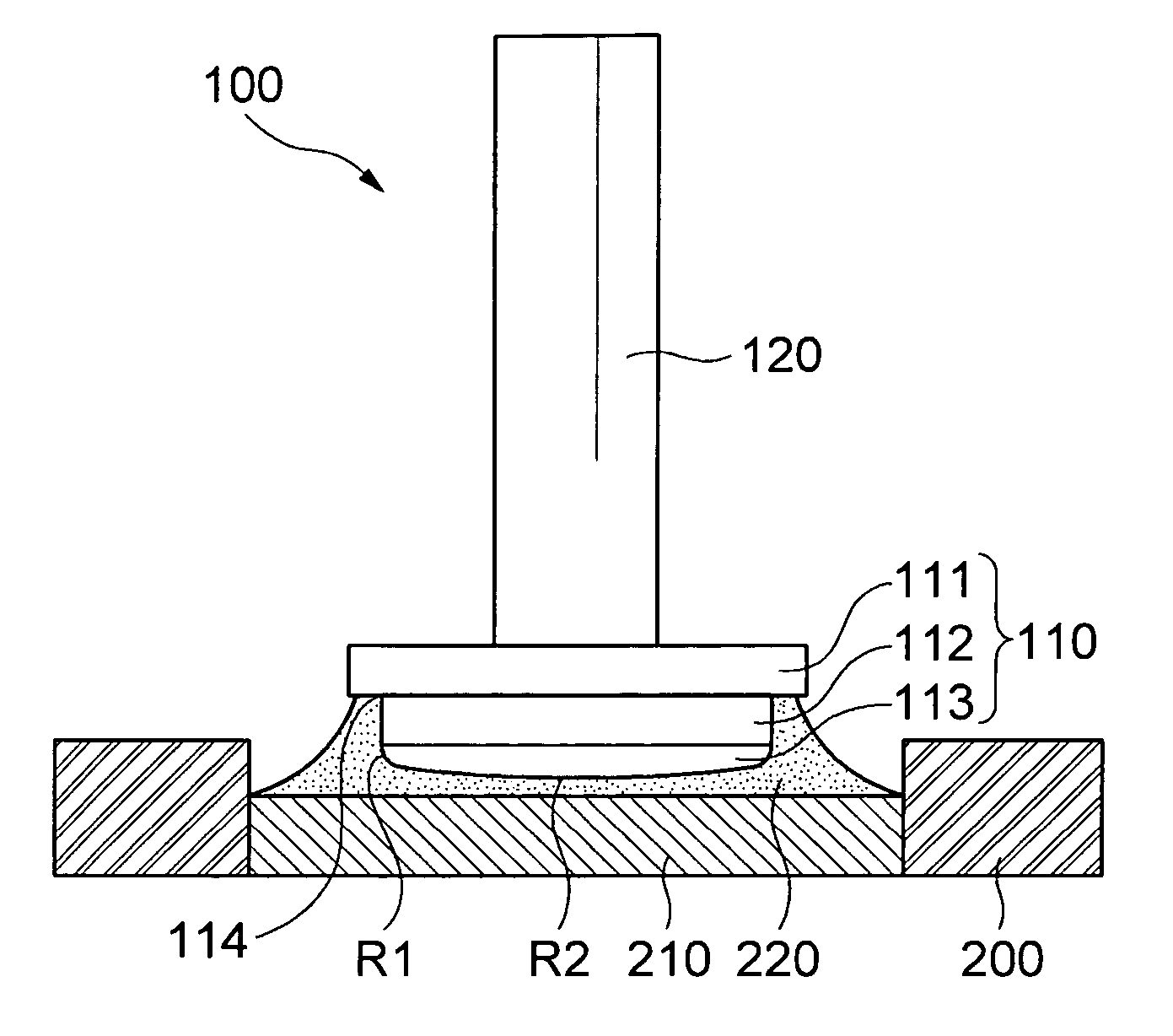
[0039]Further, FIG. 7 is a side cross-sectional view showing a configuration where a lead pin according to the present invention is mounted on a package substrate.

[0040]As shown in the drawings, a lead pin for the package substrate 100 according to the present embodiment is configured to include a head part 110 that is mounted ...


PUM


Abstract

Disclosed herein is a lead pin for a package substrate.The lead pin for the package substrate includes a cylindrical connection pin; and a head part that is formed on one end of the connection pin and has a convex round part formed on the lower end of the head part, having a step part. When the lead pin for the package substrate is mounted on the package substrate, the bulge phenomenon of a solder paste that surrounds the head part and is melted is prevented by a flange part, thereby making it possible to prevent the connection pin from being polluted and to improve a contact defect such as a short defect or the like when coupling a socket.

Description

CROSS REFERENCE TO RELATED APPLICATION[0001]This application claims the benefit of Korean Patent Application No. 10-2009-0066089, filed on Jul. 20, 2009, entitled “Lead Pin for Package Substrate”, which is hereby incorporated by reference in its entirety into this application.BACKGROUND OF THE INVENTION[0002]1. Technical Field[0003]The present invention relates to a lead pin for a package substrate, and more particularly, to a lead pin for a package substrate that includes a head part that has a round part formed on the lower end thereof, having a step part, and a connection pin that is vertically projected from the head pin.[0004]2. Description of the Related Art[0005]With the development of the electronics industry, various types of semiconductor packages have been manufactured. Recently, due to the increase in wiring density of a semiconductor package, a semiconductor package substrate in a Pin Grid Array (PGA) type in which a plurality of T-type lead pins are mounted has been wi...

Claims


Application Information

Patent Timeline
Patent Type & Authority Patents(United States)
IPC IPC(8): H01R4/02
CPCH05K3/3426H01L2924/15312H05K2201/10318H05K2201/10772Y02P70/50H01L23/495
Inventor OH, HEUNG JAELEE, KI TAEKLEE, DONG GYUJEONG, SUNG WONCHOI, JIN WON
Owner SAMSUNG ELECTRO MECHANICS CO LTD
Features
  • R&D
  • Intellectual Property
  • Life Sciences
  • Materials
  • Tech Scout
  • Unparalleled Data Quality
  • Higher Quality Content
  • 60% Fewer Hallucinations
Learn More