Check patentability & draft patents in minutes with Patsnap Eureka AI!

Method for measuring wavefront aberration

a wavefront aberration and optical system technology, applied in the direction of instruments, structural/machine measurement, printers, etc., can solve the problems of long processing time, poor reproducibility, and difficulty in precisely determining the processing center position, in both the x and y directions, to process interference fringe image data

Inactive Publication Date: 2012-07-17
CANON KK
View PDF6 Cites 0 Cited by
  • Summary
  • Abstract
  • Description
  • Claims
  • Application Information

AI Technical Summary

Problems solved by technology

This method takes a long time for processing operations such as exposure and development, so its reproducibility is poor due to errors generated in the process of resist coating and development.
For the conventional wavefront aberration measurement, and in particular, that of the LDI scheme, it is difficult to precisely determine the processing center positions, in both the X and Y directions, to process the interference fringe image data.

Method used


Image

  • Method for measuring wavefront aberration
  • Method for measuring wavefront aberration
  • Method for measuring wavefront aberration

Examples


first embodiment

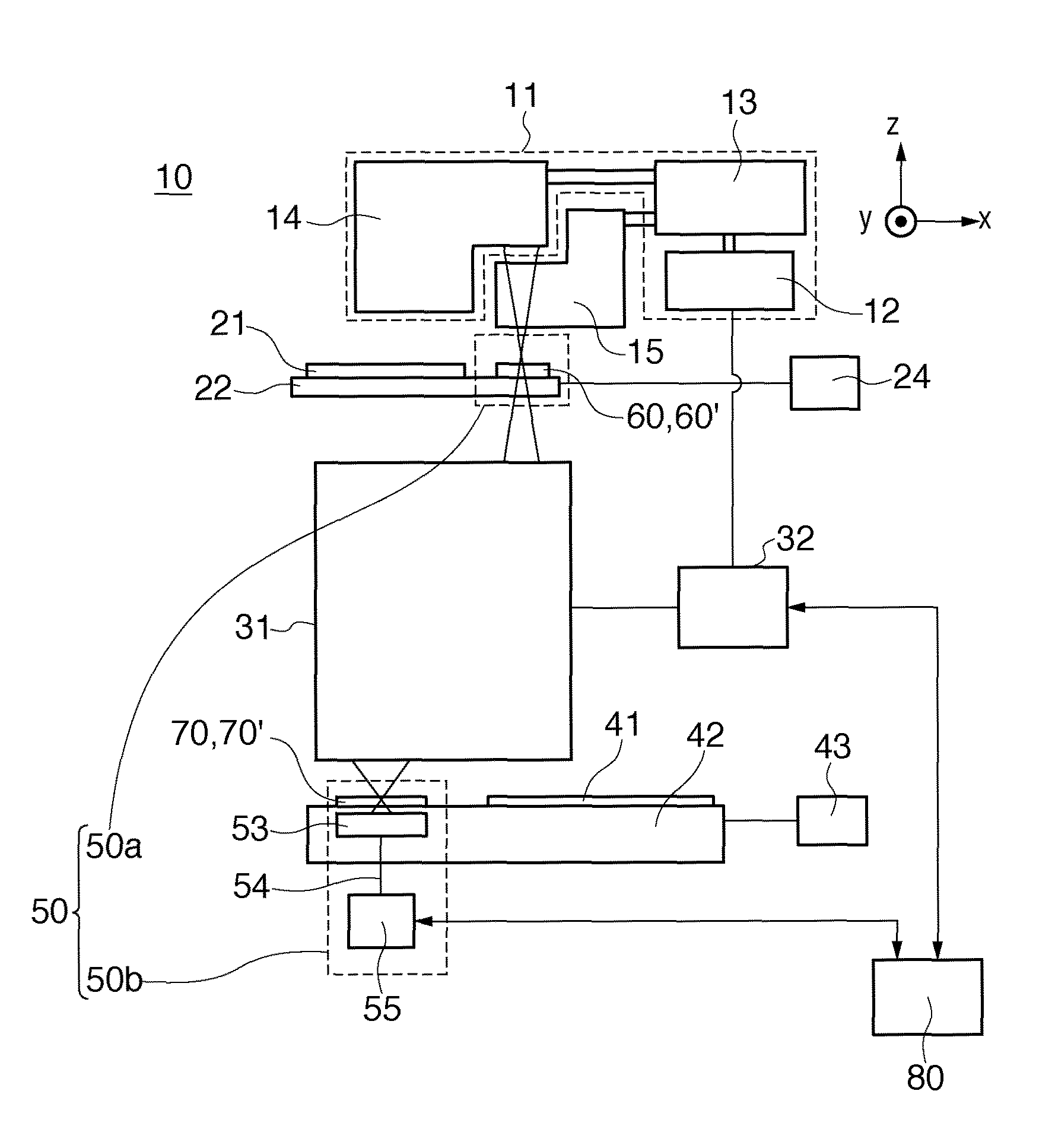
[0028]An exposure apparatus including a measurement apparatus of the PDI scheme will be explained below as the present invention. FIG. 1 is a schematic block diagram showing an exposure apparatus 10 according to an embodiment of the present invention. Note that in this specification, two orthogonal directions in a plane parallel to the image plane of a projection optical system 31 are defined as the X and Y directions.

[0029]The exposure apparatus 10 projects the pattern of an original (also called a reticle or mask) 21 onto a substrate (wafer) 41 to expose the substrate 41 by, for example, the step & scan scheme or the step & repeat scheme. The exposure apparatus 10 is suitable for lithography in which a pattern having a submicron or quarter-micron line width or less is formed.

[0030]The step & scan scheme commonly means a scheme of transferring the pattern of an original onto a substrate while scanning them with respect to the projection optical system. The step & repeat scheme comm...

second embodiment

[0088]FIG. 13 is a flowchart showing a method for measuring the wavefront aberration of the projection optical system 31 according to the This measurement method is controlled by a main control system 80. This control includes control of a measurement controller 55 by the main control system 80. The method for measuring the wavefront aberration, shown in FIG. 13, includes an X processing center detection process (step 501), Y processing center detection process (step 503), detected position correction process (step 505), and X-Y wavefront aberration calculation process (step 507).

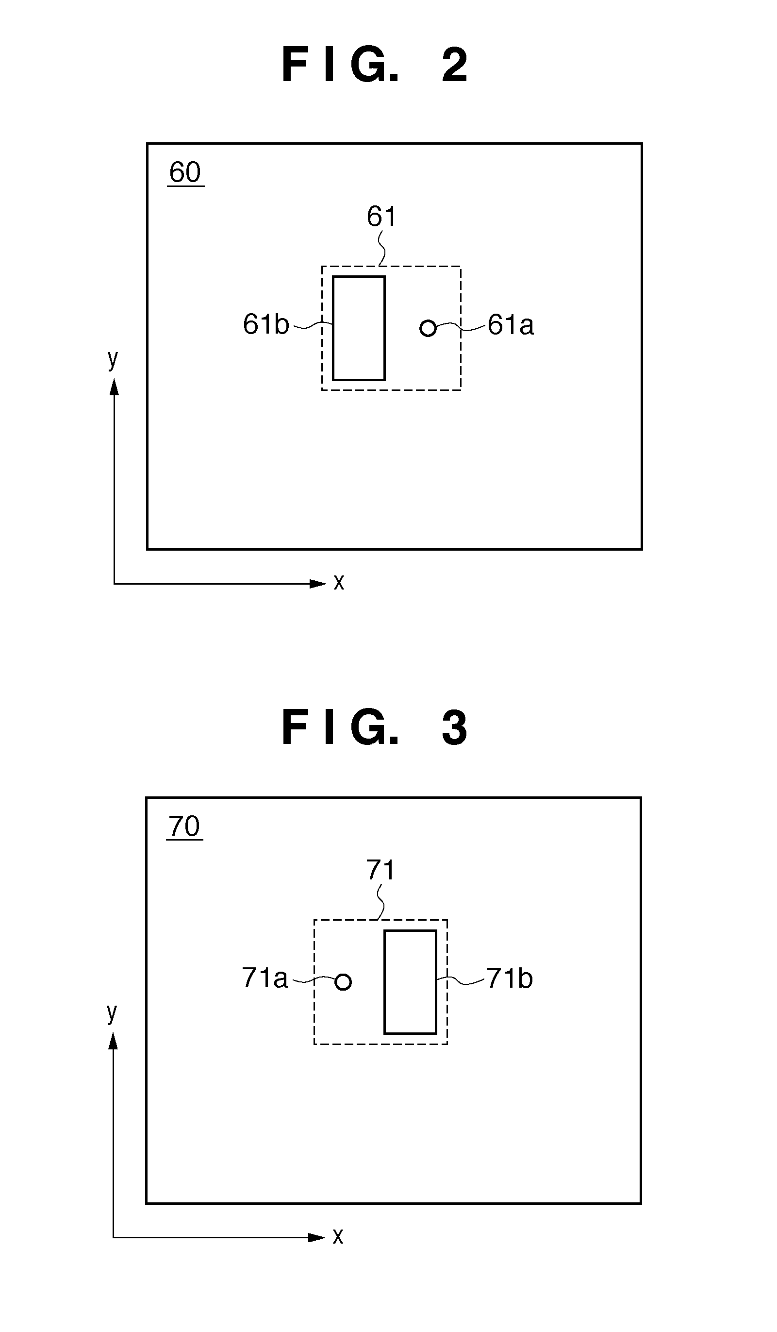
[0089]In the X processing center detection process (step 501; a first determination process), the main control system 80 acquires a plurality of X interference fringe image data having different spherical aberration amounts, and processes these image data, thereby calculating the X interference fringe processing center position.

[0090]The detailed processing in the X processing center detection process (ste...


PUM


Abstract

A method comprises determining a first processing center position to calculate a wavefront aberration of an optical system, determining a second processing center position to calculate a wavefront aberration, correcting the first processing center position in a first direction using the second processing center position in the first direction and correcting the second processing center position in a second direction using the first processing center position in the second direction.

Description

BACKGROUND OF THE INVENTION[0001]1. Field of the Invention[0002]The present invention relates to a method for measuring the wavefront aberration of an optical system.[0003]2. Description of the Related Art[0004]An exposure apparatus which transfers the pattern of an original onto a substrate has been conventionally employed in manufacturing, for example, a semiconductor device by photolithography. Since the exposure apparatus may have to precisely transfer the pattern of an original onto a substrate as the exposure target body at a predetermined magnification, it is important to use a projection optical system which has small aberrations and thus is excellent in imaging performance. The importance of such a projection optical system is great especially in recent years, in which the pattern to be transferred is becoming more sensitive to the aberration of the projection optical system in response to a demand for further advances in micropatterning of a device pattern. This makes it n...

Claims


Application Information

Patent Timeline
Patent Type & Authority Patents(United States)
IPC IPC(8): G03B27/42
CPCG01M11/0257G01M11/0271G03B27/52
Inventor YAMAMOTO, KAZUKI
Owner CANON KK
Features
  • R&D
  • Intellectual Property
  • Life Sciences
  • Materials
  • Tech Scout
  • Unparalleled Data Quality
  • Higher Quality Content
  • 60% Fewer Hallucinations
Learn More