Supercharge Your Innovation With Domain-Expert AI Agents!

Variable read latency on a serial memory bus

a serial memory bus and variable read latency technology, applied in the field of integrated circuits, can solve the problems of increasing the size, pin count, and interconnect cost of the memory device, and the time between the actual access time and the longest access time is inefficiently used as idle time,

Active Publication Date: 2012-10-16
INFINEON TECH LLC
View PDF2 Cites 15 Cited by
  • Summary
  • Abstract
  • Description
  • Claims
  • Application Information

AI Technical Summary

Benefits of technology

This approach enhances memory access efficiency by reducing idle time and maintaining low pin count, achieving variable read latency without increasing system costs or complexity.

Problems solved by technology

NOR offers eXecute In Place (XIP) capabilities and high read performance, but suffers from extremely low write and erase performance.
Any time between the actual access time and the longest access time would be inefficiently used as idle time.
However, the dedicated signal line increases the size, pin count, and interconnect cost of the memory device.

Method used


Image

  • Variable read latency on a serial memory bus
  • Variable read latency on a serial memory bus
  • Variable read latency on a serial memory bus

Examples


Embodiment Construction

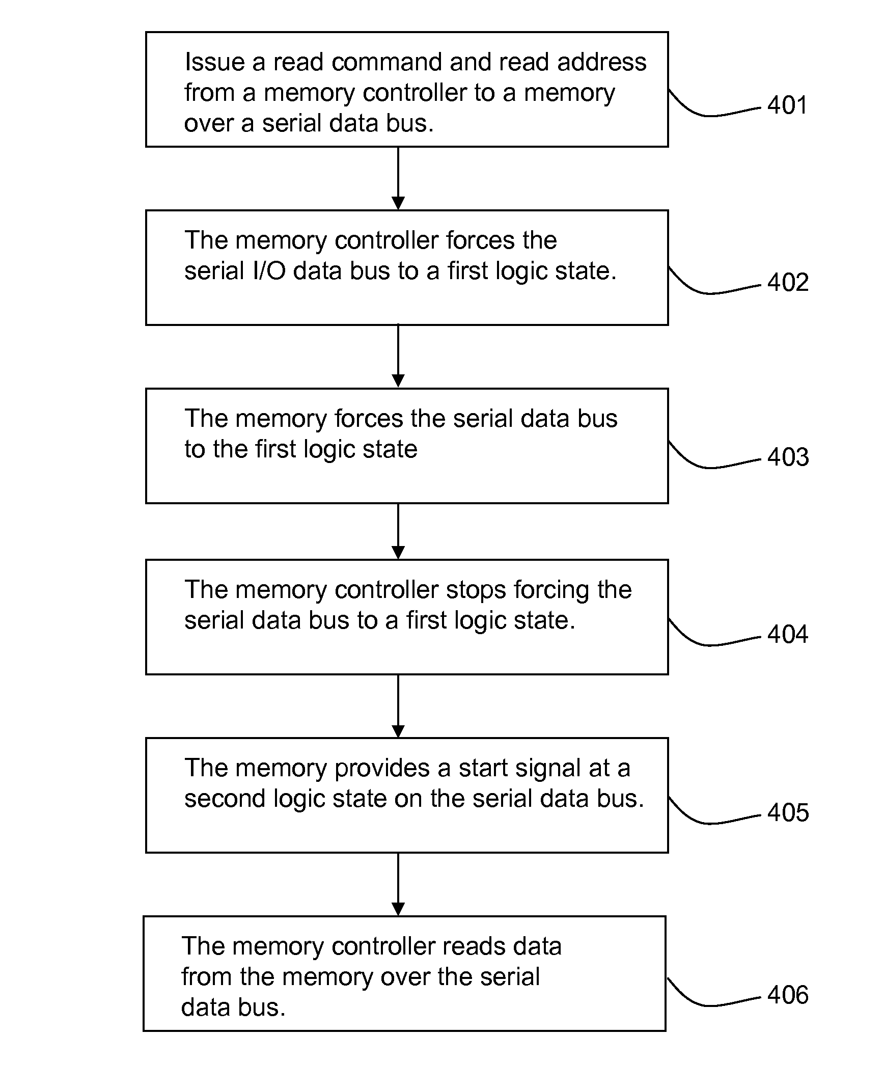
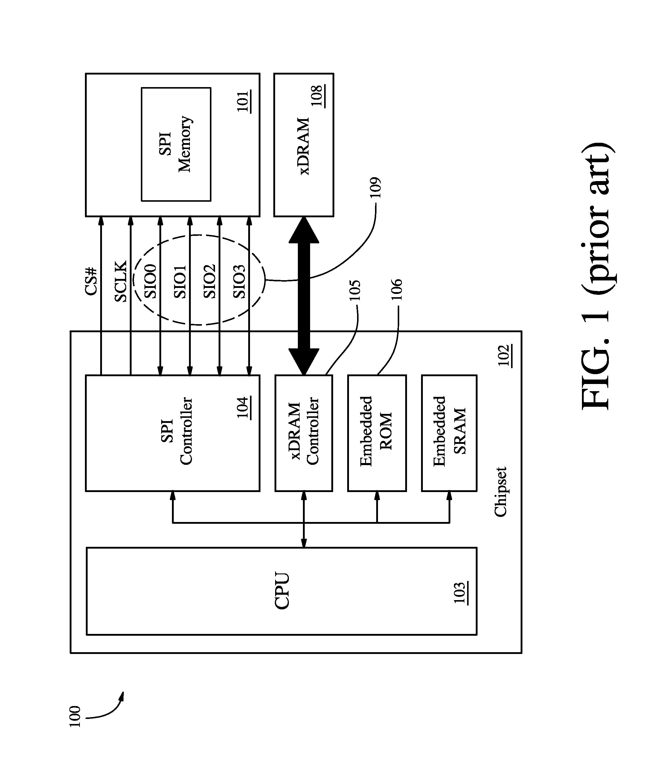
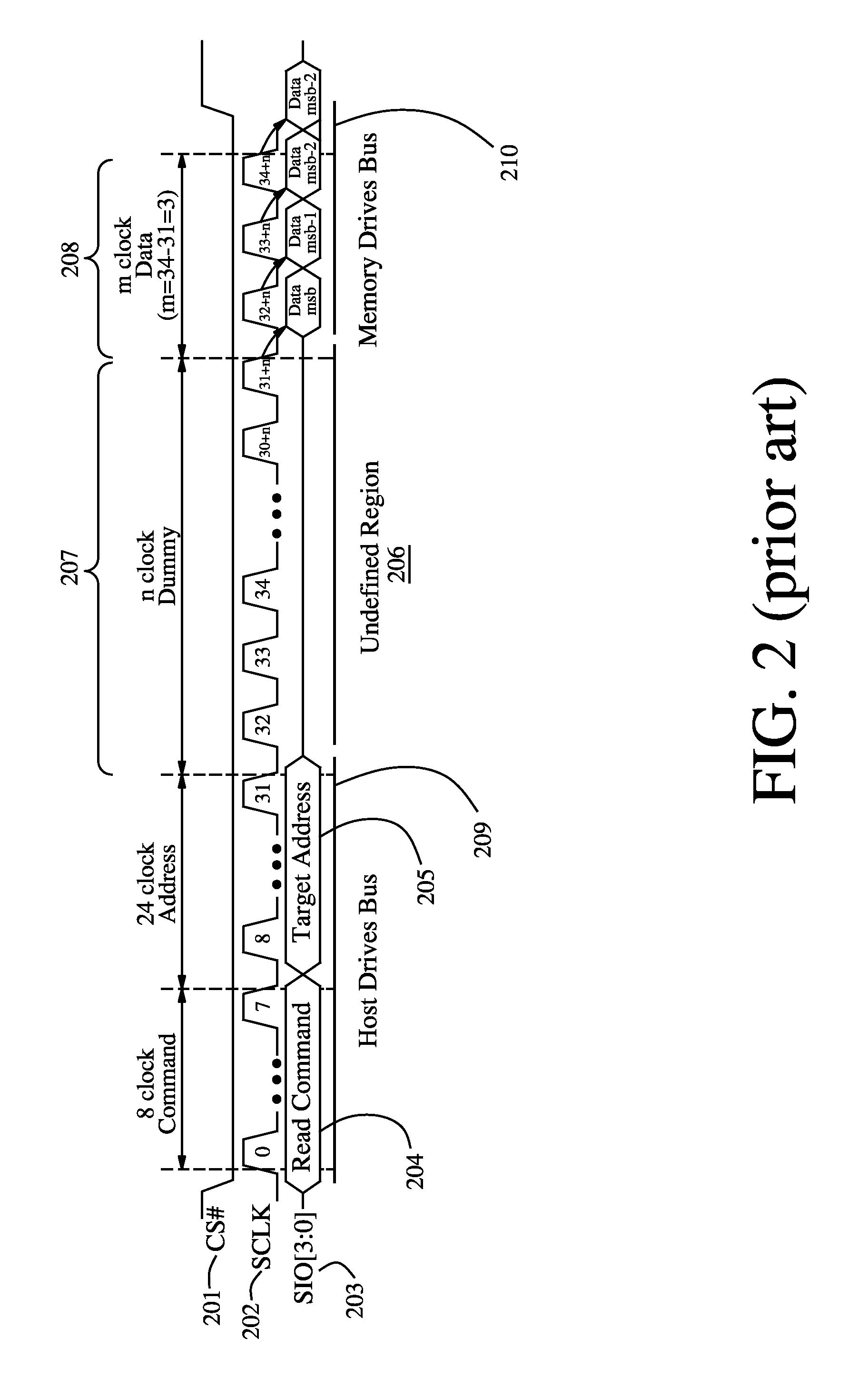
[0029]Variable latency has been successfully incorporated into the parallel burst NOR memory bus by adding a dedicated WAIT signal interface. During READ operations, the dedicated WAIT signal interface is asserted until data is ready to be output onto the data bus. Once data is available, the dedicated WAIT signal interface is deasserted and data is transferred from the memory to the host. Variable latency has had its greatest impact when incorporated on NOR-bus-based burst Pseudo Static Random Access Memory (PSRAM) devices, for which a longer latency is required for a read operation while the PSRAM device is performing an internal refresh. For these PSRAM devices, most read operations occur with a short latency during normal read operations, but the read access latency is extended when a read access collides with an ongoing internal refresh. A dedicated WAIT signal is used by many PSRAM devices to facilitate the variable latency functionality.

[0030]Reading a memory device using a v...


PUM


Abstract

One or more embodiments provide a method and system of reading data from a variable-latency memory, via a serial input / output memory data interface. The system includes a memory having a variable-latency access time, a memory controller, and a serial data bus coupling the memory controller to the memory. The memory controller communicates a Read command to the memory and forces the serial data bus low for a limited time. The memory then forces the bus low and the memory controller then releases the bus. When the memory is ready to provide data, the memory provides a high signal on the serial data bus.

Description

FIELD[0001]The present invention relates generally to integrated circuits. In particular, embodiments of the present invention relate to variable latency serial memory devices.BACKGROUND OF THE INVENTION[0002]Memory devices are typically provided as internal, semiconductor, integrated circuits in computers or other electronic devices. There are many different types of memory including random access memory (RAM), read only memory (ROM), dynamic random access memory (DRAM), synchronous dynamic random access memory (SDRAM), and flash memory.[0003]A synchronous DRAM (SDRAM) is a type of DRAM that can run at much higher clock speeds than conventional DRAM memory. SDRAM synchronizes itself with a CPU's bus and is capable of running at 100 MHZ or 133 MHZ, about three times faster than conventional FPM (Fast Page Mode) RAM, and about twice as fast EDO (Extended Data Output) DRAM and BEDO (Burst Extended Data Output) DRAM. An extended form of SDRAM that can transfer a data value on the risin...

Claims


Application Information

Patent Timeline
Patent Type & Authority Patents(United States)
IPC IPC(8): G06F3/00G06F13/00
CPCG06F13/161G06F13/4291
Inventor ZITLAW, CLIFFORD ALAN
Owner INFINEON TECH LLC
Features
  • R&D
  • Intellectual Property
  • Life Sciences
  • Materials
  • Tech Scout
  • Unparalleled Data Quality
  • Higher Quality Content
  • 60% Fewer Hallucinations
Learn More