Nonvolatile semiconductor memory having buffer layer containing nitrogen and containing carbon as main component
a buffer layer and semiconductor technology, applied in semiconductor devices, digital storage, instruments, etc., can solve the problems of unstable physical and electrical characteristics of metal oxides, less reproducibility, and the possibility of separation or peeling off of the variable resistance layer from the bottom electrod
- Summary
- Abstract
- Description
- Claims
- Application Information
AI Technical Summary
Benefits of technology
Problems solved by technology
Method used
Image

Examples
first embodiment
[0031](First Embodiment)
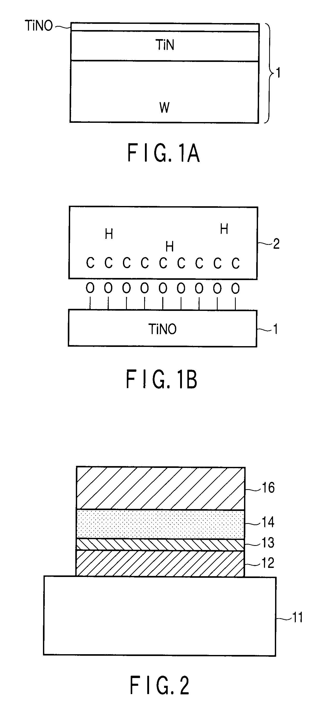
[0032]FIG. 2 is a cross-sectional view showing the element structure of a variable resistance element (nonvolatile semiconductor memory) according to a first embodiment of this invention. Symbol 11 in FIG. 2 denotes a substrate, 12 a bottom electrode, 13 a first buffer layer, 14 a variable resistance layer, and 16 a top electrode. The basic structure is the same as the conventional structure, but in this embodiment, the buffer layer 13 is formed between the variable resistance layer 14 and the bottom electrode 12 in addition to the conventional structure.
[0033]The bottom electrode 12 and top electrode 16 may be formed of a conductive material and it is sufficient if the resistance thereof is lower than that of the buffer layer 13 and variable resistance layer 14. When a voltage is applied between the bottom electrode 12 and the top electrode 16, the applied voltage is divided according to the resistances thereof. At this time, if the electrical resistances of...
second embodiment
[0046](Second Embodiment)
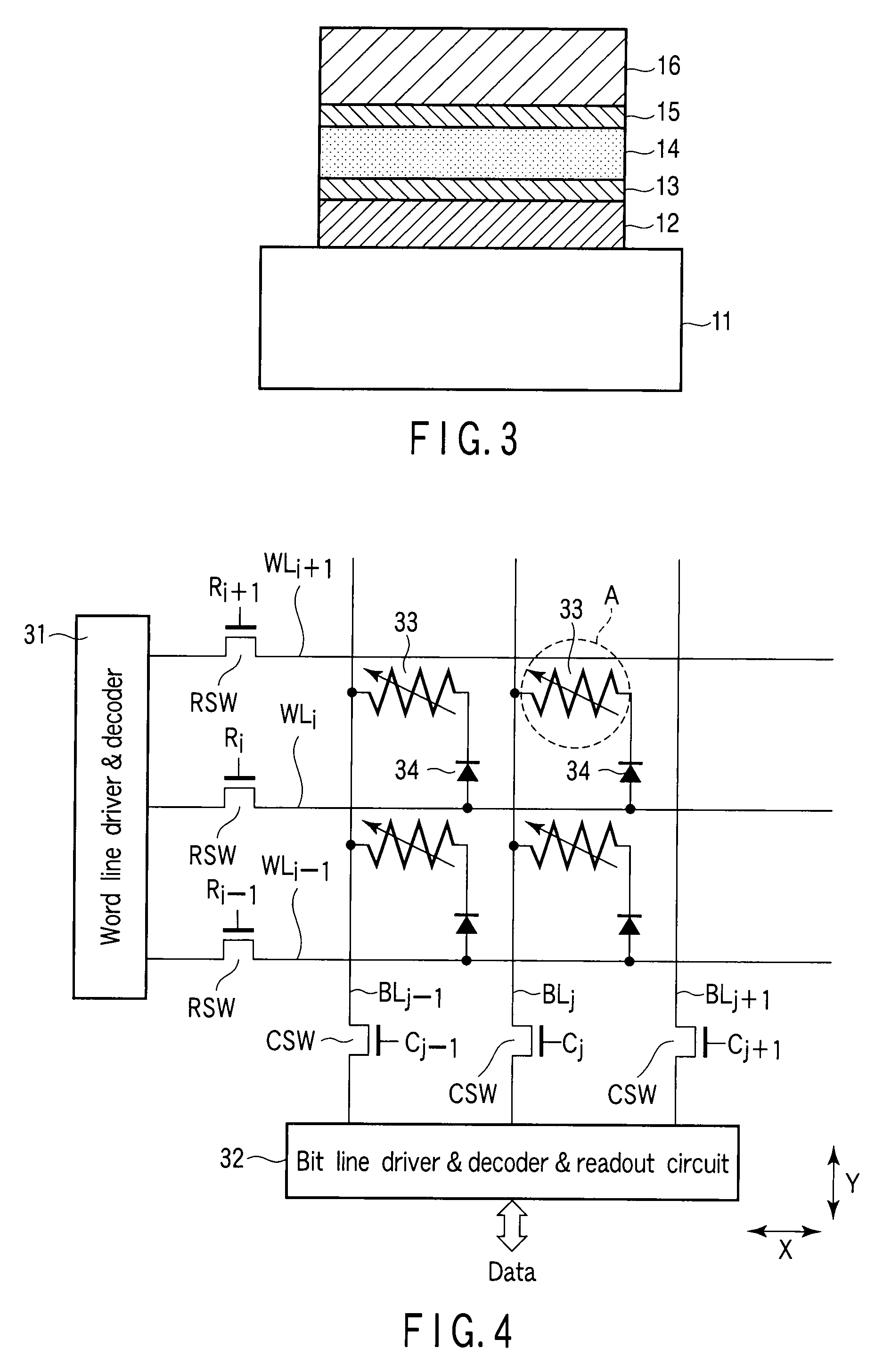
[0047]FIG. 3 is a cross-sectional view showing the element structure of a variable resistance element (nonvolatile semiconductor memory) according to a second embodiment of this invention. In this embodiment, parts that are the same as those of FIG. 1 are denoted by the same symbols and the detailed explanation thereof is omitted.
[0048]This embodiment is different from the first embodiment explained above in that not only the buffer layer is inserted between the variable resistance layer 14 and the bottom electrode 12 but also a buffer layer 15 is inserted between the variable resistance layer 14 and the top electrode 16. That is, the buffer layer 13 is formed between the variable resistance layer 14 and the bottom electrode 12 and the buffer layer 15 is formed between the variable resistance layer 14 and the top electrode 16. The buffer layer 15 may be formed of the same material as that of the buffer layer 13.
[0049]With the above structure, it is of course...
third embodiment
[0050](Third Embodiment)
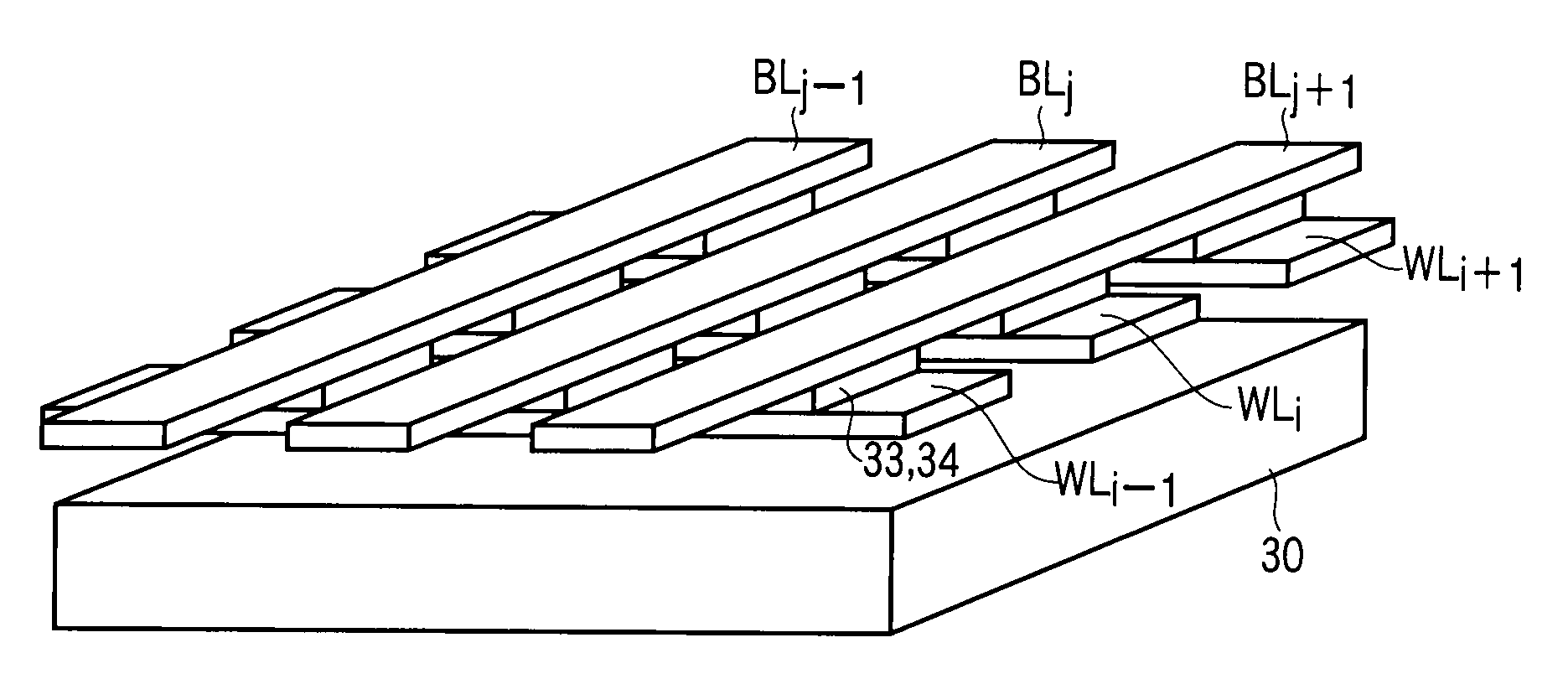
[0051]FIG. 4 is a diagram showing the circuit configuration of a cross-point type nonvolatile semiconductor storage device according to a third embodiment of this invention.
[0052]A plurality of word lines WL (WLi−1, WLi, WLi+1) and a plurality of bit lines BL (BLj−1, BLj, BLj+1) are arranged in parallel, the word lines WL extend in an X direction and the bit lines BL extend in a Y direction. In FIG. 4, only three word lines and bit lines are shown, but in practice, a larger number of word lines WL and bit lines BL are arranged.
[0053]One-side ends of the word lines WL are connected to a word line driver & decoder 31 via MOS transistors RSW acting as selection switches. One-side ends of the bit lines BL are connected to a bit line driver & read circuit 32 via MOS transistors CSW acting as selection switches.
[0054]The gates of the MOS transistors RSW are respectively supplied with selection signals R (Ri−1, Ri, Ri+1) used to select one word line (row). The gates...
PUM
 Abstract
Description
Claims
Application Information
 - R&D
- Intellectual Property
- Life Sciences
- Materials
- Tech Scout
- Unparalleled Data Quality
- Higher Quality Content
- 60% Fewer Hallucinations
Browse by: Latest US Patents, China's latest patents, Technical Efficacy Thesaurus, Application Domain, Technology Topic, Popular Technical Reports.
© 2025 PatSnap. All rights reserved.Legal|Privacy policy|Modern Slavery Act Transparency Statement|Sitemap|About US| Contact US: help@patsnap.com