Check patentability & draft patents in minutes with Patsnap Eureka AI!

Manufacturing method, surface-emitting laser device, surface-emitting laser array, optical scanner, and image forming apparatus

a laser array and surface-emitting technology, applied in semiconductor lasers, instruments, electrographic processes, etc., can solve the problems of unable to obtain the reliability of the laser device, and the inability to meet the requirements of the laser devi

Active Publication Date: 2013-04-09
RICOH KK
View PDF43 Cites 4 Cited by
  • Summary
  • Abstract
  • Description
  • Claims
  • Application Information

AI Technical Summary

Benefits of technology

The method significantly enhances the reliability and service life of surface-emitting laser devices by preventing water penetration and oxidation, improving their performance in high-temperature and high-humidity conditions.

Problems solved by technology

Meanwhile, since the surface-emitting laser device is susceptible to humidity (water), various countermeasures have been taken (see, for example, Patent Documents 1 through 3).
With the countermeasures disclosed in Patent Documents 1 through 3, however, demanded reliability may not be obtained.

Method used


Image

  • Manufacturing method, surface-emitting laser device, surface-emitting laser array, optical scanner, and image forming apparatus
  • Manufacturing method, surface-emitting laser device, surface-emitting laser array, optical scanner, and image forming apparatus
  • Manufacturing method, surface-emitting laser device, surface-emitting laser array, optical scanner, and image forming apparatus

Examples


Embodiment Construction

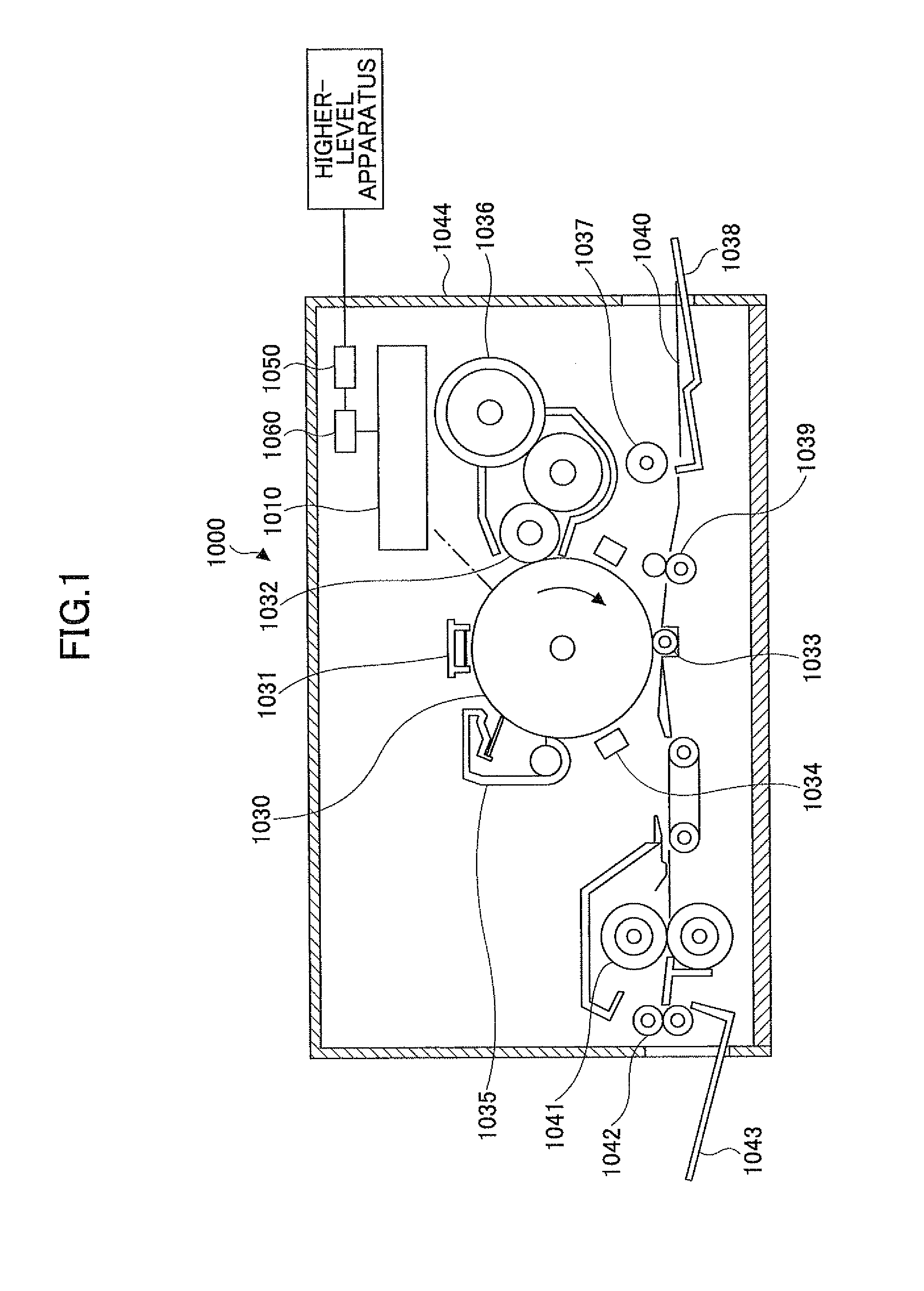
[0034]Next, an embodiment of the present invention is described below with reference to FIGS. 1 through 12. FIG. 1 shows the schematic configuration of a laser printer 1000 serving as an image forming apparatus according to the embodiment.

[0035]The laser printer 1000 has an optical scanner 1010, a photosensitive drum 1030, an electrifying charger 1031, a developing roller 1032, a transfer charger 1033, a charge removing unit 1034, a cleaning unit 1035, a toner cartridge 1036, a sheet feeding roller 1037, a sheet feeding tray 1038, a pair of resist rollers 1039, a fixing roller 1041, a sheet discharging roller 1042, a sheet catching tray 1043, a communication control unit 1050, a printer control unit 1060 that collectively controls the above units, and the like. Note that these units are accommodated at predetermined positions in a printer housing 1044.

[0036]The communication control unit 1050 controls interactive communications with a higher-level apparatus (for example, a personal ...


PUM


Abstract

A manufacturing method for manufacturing a surface-emitting laser device includes the steps of forming a laminated body in which a lower reflecting mirror, a resonator structure including an active layer, and an upper reflecting layer having a selective oxidized layer are laminated on a substrate; etching the laminated body to form a mesa structure having the selective oxidized layer exposed at side surfaces thereof; selectively oxidizing the selective oxidized layer from the side surfaces of the mesa structure to form a constriction structure in which a current passing region is surrounded by an oxide; forming a separating groove at a position away from the mesa structure; passivating an outermost front surface of at least a part of the laminated body exposed when the separating groove is formed; and coating a passivated part with a dielectric body.

Description

TECHNICAL FIELD[0001]The present invention relates to manufacturing methods, surface-emitting laser devices, surface-emitting laser arrays, optical scanners, and image forming apparatuses and, more specifically, to a manufacturing method for manufacturing a surface-emitting laser device, a surface-emitting laser device that emits laser light in a direction perpendicular to a substrate, a surface-emitting laser array, an optical scanner having the surface-emitting laser device or the surface-emitting laser array, and an image forming apparatus having the optical scanner.BACKGROUND ART[0002]A vertical cavity surface-emitting laser (VCSEL) device is a semiconductor laser device that emits light in a direction perpendicular to a substrate and has received attention due to its (1) competitive price, (2) low power consumption, (3) small size and high performance, and (4) ease of two-dimensional integration when compared with an end-surface-emitting semiconductor laser device that emits li...

Claims


Application Information

Patent Timeline
Patent Type & Authority Patents(United States)
IPC IPC(8): H01S5/00
CPCH01S5/423H01S5/18361H01S5/0202H01S5/18311H01S5/3202H01S2301/173H01S2301/176
Inventor SHOUJI, HIROYOSHISATO, SHUNICHIISHII, TOSHIHIROMAKITA, KENGOHAYASHI, MASAHIROSASAKI, TOSHIHIDEITOH, AKIHIRO
Owner RICOH KK
Features
  • R&D
  • Intellectual Property
  • Life Sciences
  • Materials
  • Tech Scout
  • Unparalleled Data Quality
  • Higher Quality Content
  • 60% Fewer Hallucinations
Learn More