Semiconductor package having substrate for high speed semiconductor package
a technology of semiconductor and substrate, which is applied in the direction of semiconductor devices, semiconductor/solid-state device details, electrical devices, etc., can solve problems such as data processing speed degradation
- Summary
- Abstract
- Description
- Claims
- Application Information
AI Technical Summary
Benefits of technology
Problems solved by technology
Method used
Image

Examples
Embodiment Construction
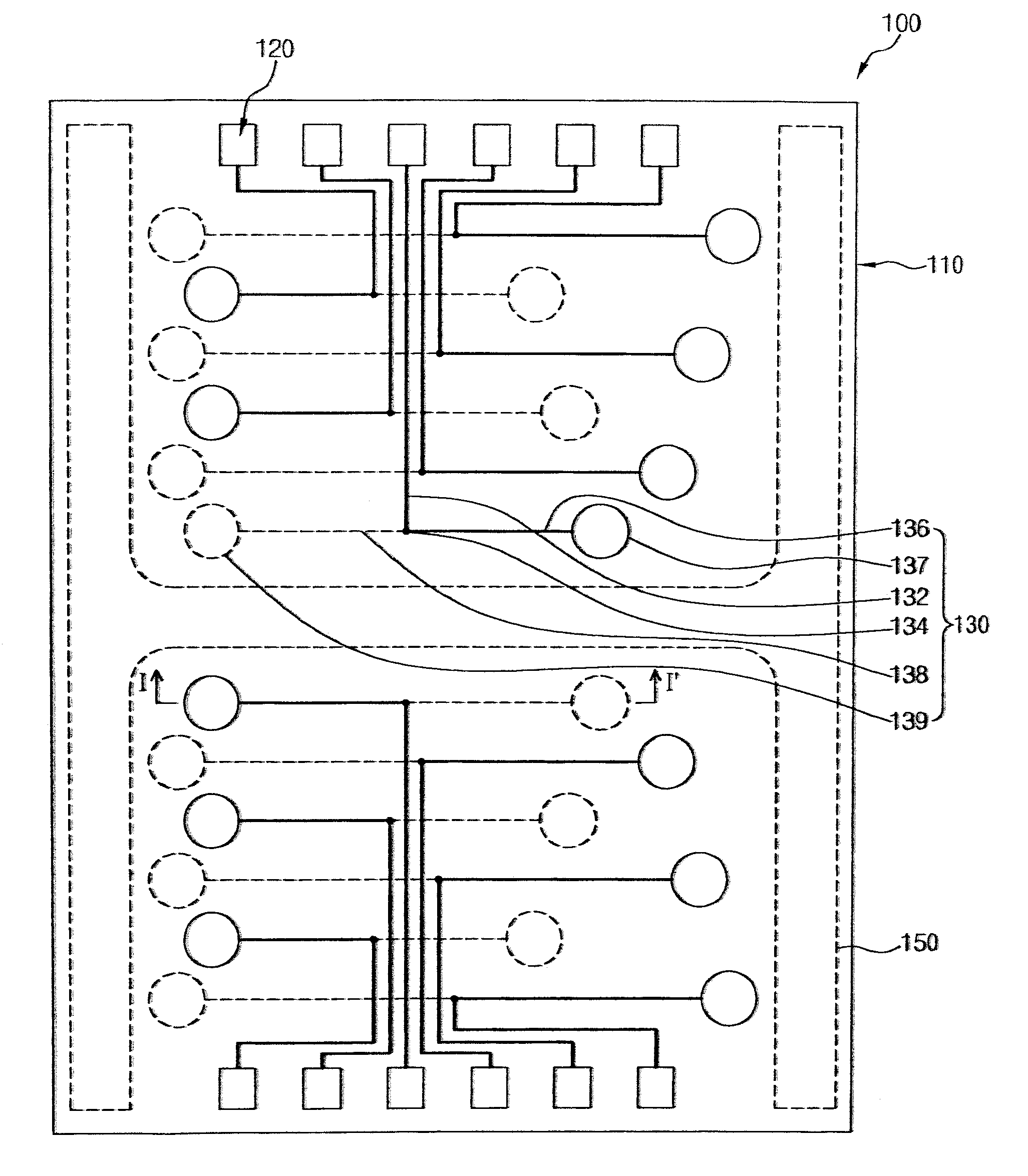
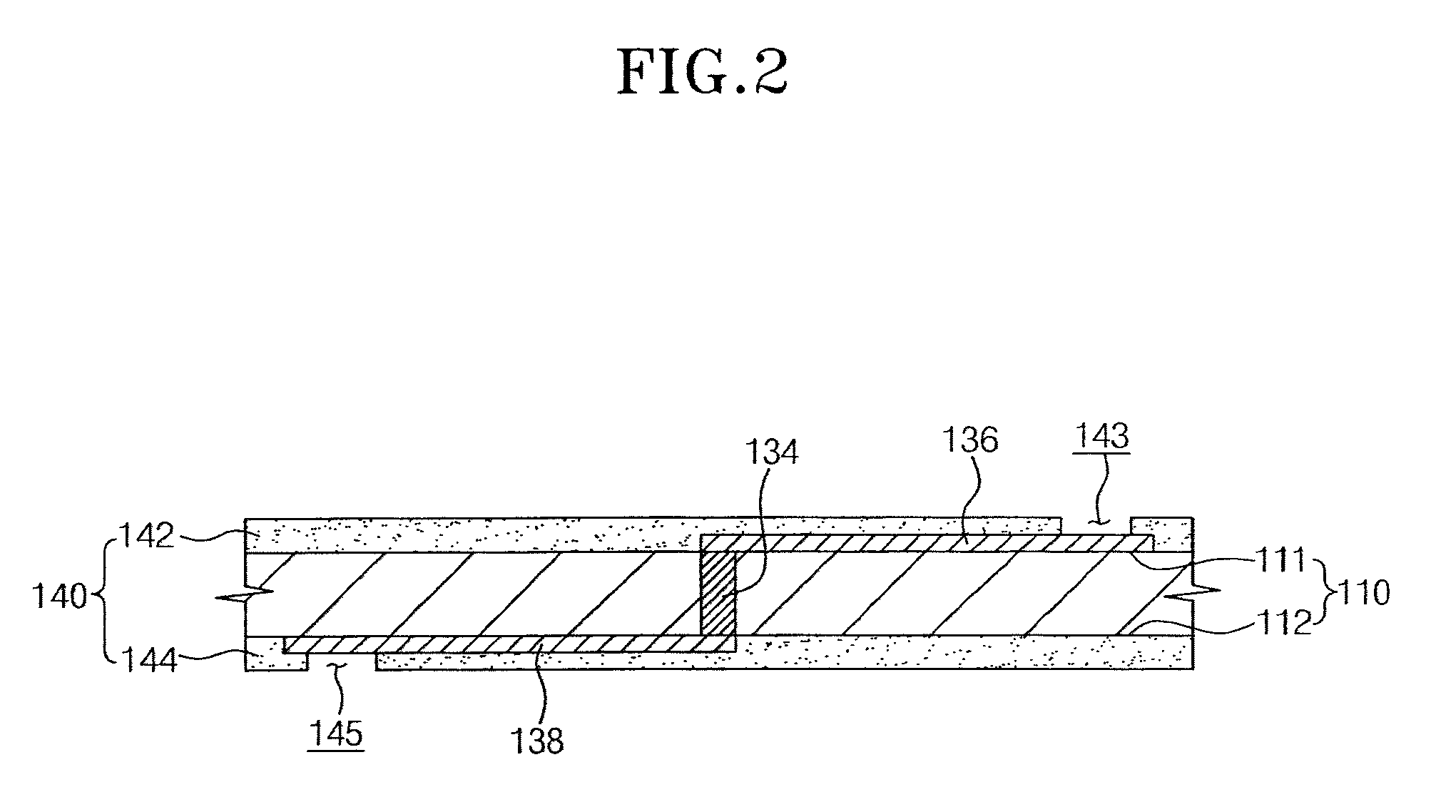
[0036]FIG. 1 is a plan view illustrating the upper surface of a substrate for a semiconductor package in accordance with an embodiment of the present invention. FIG. 2 is a sectional view taken along the line I-I′ of FIG. 1. FIG. 3 is a bottom view illustrating the lower surface of the substrate for a semiconductor package, which faces away from the upper surface shown in FIG. 1.
[0037]Referring to FIGS. 1 through 3, a substrate 100 for a semiconductor package includes a substrate body 110, connection pads 120, and signal lines 130. The reference numeral 150 in FIG. 1 designates a power line through which power is supplied.
[0038]In the present embodiment, the substrate body 110, for example, may be a printed circuit board (PCB) having a planar shape. As shown in FIG. 2, the substrate body 110 has a first surface 111 and a second surface 112 opposite the first surface 111. Alternatively, the substrate body 110 may be a flexible substrate, which can be bent.
[0039]The connection pads 12...
PUM
 Abstract
Description
Claims
Application Information
 - R&D
- Intellectual Property
- Life Sciences
- Materials
- Tech Scout
- Unparalleled Data Quality
- Higher Quality Content
- 60% Fewer Hallucinations
Browse by: Latest US Patents, China's latest patents, Technical Efficacy Thesaurus, Application Domain, Technology Topic, Popular Technical Reports.
© 2025 PatSnap. All rights reserved.Legal|Privacy policy|Modern Slavery Act Transparency Statement|Sitemap|About US| Contact US: help@patsnap.com