Check patentability & draft patents in minutes with Patsnap Eureka AI!

Optical receiver circuit

a receiver circuit and optical receiver technology, applied in the field of optical receiver circuits, can solve the problems of high-frequency noise leakage through power supply wiring, inability to reduce high-frequency noise leakage through the power supply wiring, and significant oscillation phenomena, and achieve the effect of reducing the oscillation phenomenon

Inactive Publication Date: 2013-07-02
HITACHI LTD
View PDF7 Cites 2 Cited by
  • Summary
  • Abstract
  • Description
  • Claims
  • Application Information

AI Technical Summary

Benefits of technology

This configuration effectively reduces high-frequency noise leakage and oscillation phenomena by ensuring the substrate supply interval between the two wiring regions is large enough to fully attenuate noise in the AC manner, improving the stability of the optical receiver circuit.

Problems solved by technology

However, when the optical receiver circuit is connected with the peripheral mounting system by bonding wires, the power supply potential in the optical receiver circuit is not grounded in an alternating current (AC) manner in a high-frequency region because the impedance of the bonding wire is high in a high-frequency region.
Accordingly, when the power supply wiring for the preamplifier and that for the main amplifier are used in common, high-frequency noise leak through the power supply wiring cannot be reduced.
The oscillation phenomenon becomes significant as the gain of the optical receiver circuit increases and as the impedance of the bonding wire connected with a power supply pad and a ground potential pad of the optical receiver circuit increases, which causes a problem, in particular, in the case of a broadband and high-gain optical receiver circuit of a gigabit order.
However, the inventors of the present application have found that it is sometimes difficult to reduce the aforementioned oscillation phenomenon occurring due to the high-frequency noise leak through the ground potential wiring and the substrate to which the potential of the ground potential wiring is supplied.

Method used


Image

  • Optical receiver circuit
  • Optical receiver circuit
  • Optical receiver circuit

Examples


first embodiment

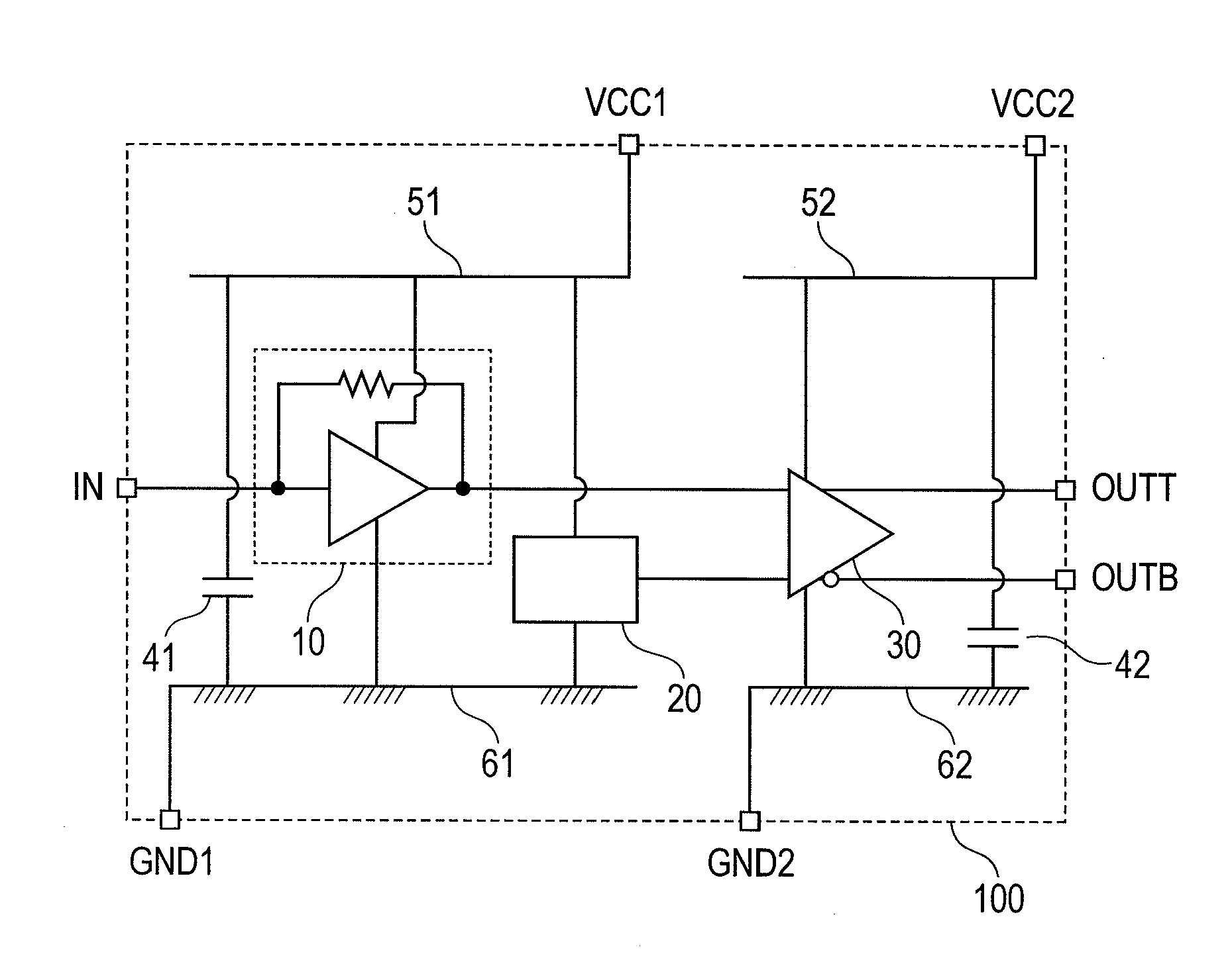
[0056]FIG. 1 shows a first embodiment of the optical receiver circuit using the present invention. The optical receiver circuit 100 of the present embodiment comprises: a preamplifier 10 to receive, as an input, a current signal outputted by a photoelectric conversion circuit photodiode 200 that receives an optical signal shown in FIG. 3 and converts it into a current signal, and to convert the current signal into a voltage signal; a reference voltage generating circuit 20 to generate a DC voltage necessary for single-to-differential conversion; and a main amplifier 30 to output a differential voltage signal by amplifying the difference between the voltage signals outputted by the preamplifier 10 and the reference voltage generating circuit 20. The preamplifier 10 and the reference voltage generating circuit 20 are connected with first ground potential wiring 61 and first power supply wiring 51, which are used in common, and the main amplifier 30 is connected with second ground pote...

second embodiment

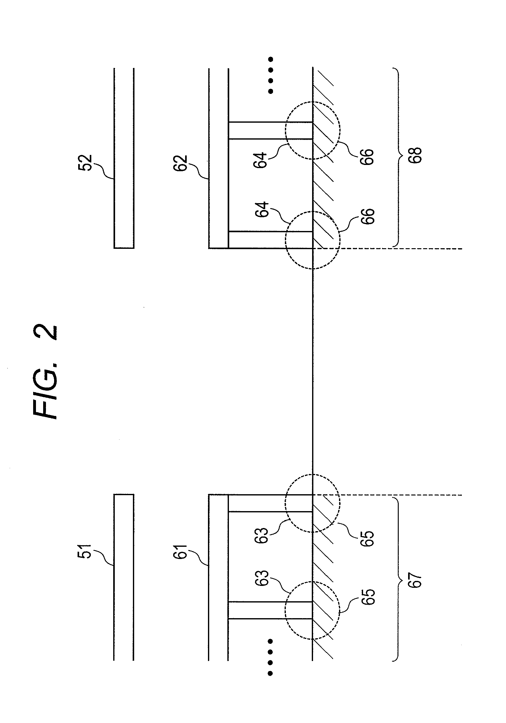
[0065]FIG. 10 shows a second embodiment of the optical receiver circuit using the present invention. The present embodiment is different from the first embodiment in that: whereas the optical receiver circuit 100 of the first embodiment is provided with one circuit to generate reference current and one current output circuit 70, the optical receiver circuit 100 of the present embodiment shown in FIG. 10 is provided with a first circuit to generate reference current and a first current output circuit 71, which are connected with the first ground potential wiring 61 and the first power supply wiring 51 and are formed in the first region where elements are formed 67 shown in FIG. 2, and a second circuit to generate reference current and a second current output circuit 72, which are connected with the second ground potential wiring 62 and the second power supply wiring 52 and are formed in the second region where elements are formed 68 shown in FIG. 2. The first circuit to generate refe...

third embodiment

[0070]FIG. 12 shows a third embodiment of the optical receiver circuit using the present invention. The present embodiment is different from the second embodiment in that a second current output circuit 82 is only connected with the second power supply wiring and the second ground potential wiring and is formed in the second region where elements are formed 68. A circuit to generate reference current 80 and a first current output circuit 81 are connected with the first power supply wiring 51 and the first ground potential wiring 61 and are formed in the first region where elements are formed 67. The first current output circuit 81 has a function of outputting a reference current to the preamplifier 10, the reference voltage generating circuit 20, and other circuits that are connected with the first power supply wiring 51 and the first ground potential wiring 61 and are formed in the first region where elements are formed 67. The second current output circuit 82 has a function of out...


PUM


Abstract

An optical receiver circuit is configured as follows: a preamplifier and a reference voltage generating circuit are connected with a first ground potential wiring and a first power supply wiring, which are used in common, and are formed in a first region where elements are formed on a substrate to which the potential of the first ground potential wiring is supplied; a main amplifier is connected with a second ground potential wiring and a second power supply wiring, which are separated from the first ground potential wiring and the first power supply wiring, and is formed in a second region where elements are formed on the substrate to which the potential of the second ground potential wiring is supplied; and a substrate supply interval where a first substrate supply position at which the potential of the first ground potential wiring is supplied and a second substrate supply position at which the potential of the second ground potential wiring is supplied are closest to each other is large to an extent where a substrate permeability characteristic, in which noise is fully attenuated in an alternating current (AC) manner, is obtained.

Description

CLAIM OF PRIORITY[0001]The present application claims priority from Japanese patent application JP 2010-014985 filed on Jan. 27, 2010, the content of which is hereby incorporated by reference into this application.FIELD OF THE INVENTION[0002]The present invention relates to an optical receiver circuit for converting a current signal, which has been generated by a photoelectric conversion circuit, into a voltage signal or a differential voltage signal, and more particularly, to an optical receiver circuit of a gigabit order.BACKGROUND OF THE INVENTION[0003]As a technique for reducing high-frequency noise leak through power supply wiring in an optical receiver circuit, there has conventionally been a technique in which a main amplifier is supplied with a power supply voltage by second power supply wiring separated from first power supply wiring by which a preamplifier is supplied with the power supply voltage (for example, see JP-A-2003-332855).[0004]In addition, as a technique for re...

Claims


Application Information

Patent Timeline
Patent Type & Authority Patents(United States)
IPC IPC(8): H03F3/08H01J43/00H01J43/30
CPCH03F3/087
Inventor MATSUDA, SHOUGOYOSHIOKA, HIROYUKISATOMURA, RYUICHITAKAHASHI, HIDEYUKIGOTO, AKIHIKO
Owner HITACHI LTD
Features
  • R&D
  • Intellectual Property
  • Life Sciences
  • Materials
  • Tech Scout
  • Unparalleled Data Quality
  • Higher Quality Content
  • 60% Fewer Hallucinations
Learn More