Supercharge Your Innovation With Domain-Expert AI Agents!

Semiconductor device having a vertical cavity surface emitting laser (VCSEL) and a protection diode integrated therein and having reduced capacitance to allow the VCSEL to achieve high operating speeds

a technology of vertical cavity surface and emitting laser, which is applied in the direction of semiconductor lasers, lasers, solid-state devices, etc., can solve the problems of reducing the operating speed of the laser diode, reducing the area a to reduce csub>d /sub>, and increasing the vulnerability of the vcsel to electrostatic discharge damage, etc., to achieve high speed, reduce the capacitance of the protection diode, and reduce the capacitance of the protection di

Active Publication Date: 2013-07-16
AVAGO TECH INT SALES PTE LTD
View PDF9 Cites 3 Cited by
  • Summary
  • Abstract
  • Description
  • Claims
  • Application Information

AI Technical Summary

Benefits of technology

The design allows VCSELs to operate at higher speeds by minimizing capacitance, thereby increasing the damage threshold and data rate while effectively protecting against ESD events.

Problems solved by technology

Decreasing the size of the aperture, however, makes the VCSEL increasingly susceptible to electrostatic discharge (ESD) damage.
One of the problems associated with integrating the protection diode together with the laser diode in the same semiconductor device is that the inclusion of the protection diode introduces capacitance, which decreases the operating speed of the laser diode.
Decreasing area A to reduce Cd is not desirable because a small area A leads to a high thermal resistance and high current density.
The high thermal resistance will lead to rapid temperature rise during an ESD event and result in a low damage threshold.
On the other hand, increasing the area, A, of the protection diode increases the damage threshold voltage of the laser diode, but also increases the amount of capacitance that is introduced by the protection diode, which limits the operating speed, or the data rate, of the laser diode.
Although the design described in U.S. Pat. No. 6,185,240 can be configured such that Cd is relatively small, the design cannot be used in the common VCSEL configuration described above because the cathode (n-side) of the VCSEL and diode are always connected through the substrate.
Consequently, the substrate cannot be a conducting substrate.

Method used


Image

  • Semiconductor device having a vertical cavity surface emitting laser (VCSEL) and a protection diode integrated therein and having reduced capacitance to allow the VCSEL to achieve high operating speeds
  • Semiconductor device having a vertical cavity surface emitting laser (VCSEL) and a protection diode integrated therein and having reduced capacitance to allow the VCSEL to achieve high operating speeds
  • Semiconductor device having a vertical cavity surface emitting laser (VCSEL) and a protection diode integrated therein and having reduced capacitance to allow the VCSEL to achieve high operating speeds

Examples


Embodiment Construction

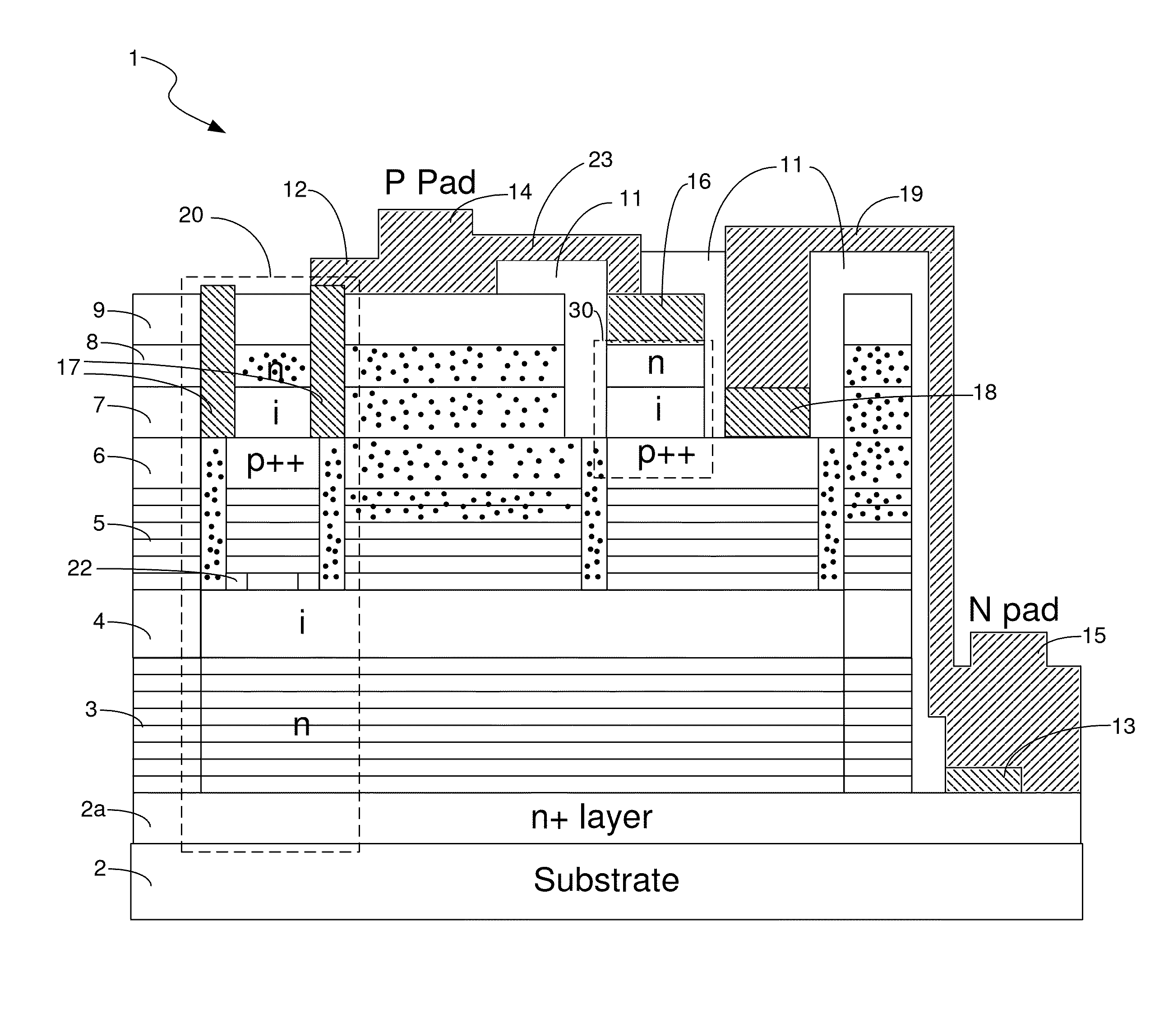
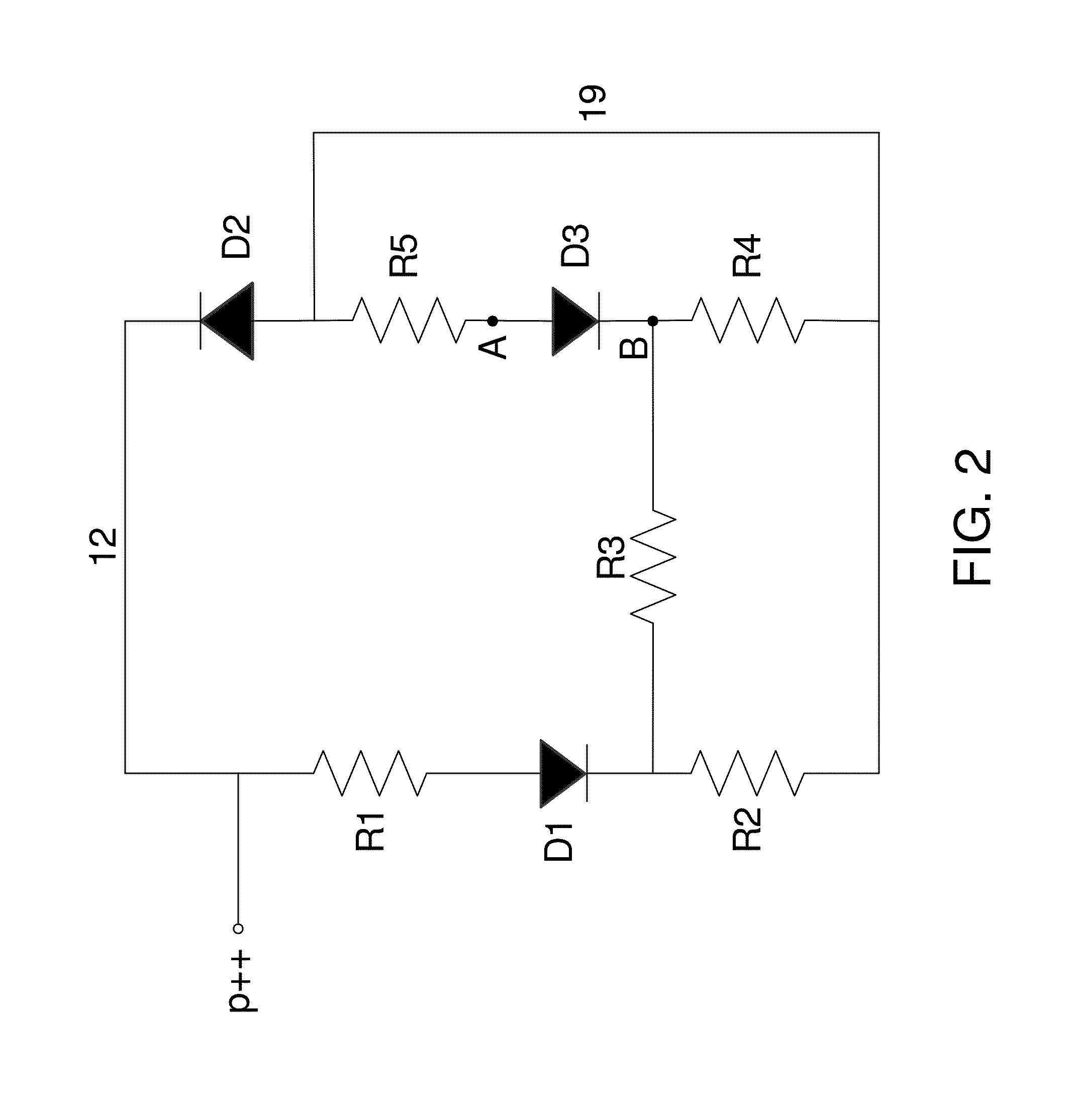
[0014]The invention is directed to a semiconductor device having a VCSEL and a protection diode integrated therein. An additional intrinsic (i) layer is included in the semiconductor device. The inclusion of the additional i layer allows the width, d, of the depletion region of the protection diode to be increased, which reduces the amount of capacitance, Cd, that is introduced by the protection diode. Reducing Cd allows the VCSEL to operate at higher speeds. An illustrative, or exemplary, embodiment will now be described with reference to FIGS. 1-3, in which like reference numerals represent like features, elements or components.

[0015]FIG. 1 illustrates a cross-sectional view of the semiconductor device 1 in accordance with an illustrative, or exemplary, embodiment. FIG. 3 illustrates a top plan view of a portion of the semiconductor device 1 shown in FIG. 1. The semiconductor device 1 has an n+ substrate 2 having a n+ layer 2a disposed thereon, a lower n-type distributed Bragg ref...


PUM


Abstract

A semiconductor device is provided that has a VCSEL and a protection diode integrated therein and that has an additional intrinsic layer. The inclusion of the additional intrinsic layer increases the width of the depletion region of the protection diode, which reduces the amount of capacitance that is introduced by the protection diode. Reducing the amount of capacitance that is introduced by the protection diode allows the VCSEL to operate at higher speeds.

Description

TECHNICAL FIELD OF THE INVENTION[0001]The invention relates to vertical cavity surface emitting lasers (VCSELs). More particularly, the invention relates to a semiconductor device having a VCSEL and a protection diode integrated therein and having reduced capacitance to allow the VCSEL to achieve high operating speeds.BACKGROUND OF THE INVENTION[0002]VCSELs are widely used as light sources for optical interconnect devices, storage area networks, and sensors. In order to enable VCSELs to operate at increasingly higher speeds, or data rates, the aperture sizes must be made increasingly smaller. Decreasing the size of the aperture, however, makes the VCSEL increasingly susceptible to electrostatic discharge (ESD) damage. The ESD damage threshold for VCSELs is commonly characterized by models such as the human body model (HBM) and the machine model (MM). For a VCSEL aperture diameter in the range of 5-10 micrometers (microns), the HBM damage threshold voltage is typically in the range o...

Claims


Application Information

Patent Timeline
Patent Type & Authority Patents(United States)
IPC IPC(8): H01S5/00
CPCH01S5/183H01L25/167H01S5/0261H01S5/06825H01S5/0425H01S5/18308H01L2924/0002H01S5/04257H01L2924/00
Inventor MURTY, RAMANA M. V.
Owner AVAGO TECH INT SALES PTE LTD
Features
  • R&D
  • Intellectual Property
  • Life Sciences
  • Materials
  • Tech Scout
  • Unparalleled Data Quality
  • Higher Quality Content
  • 60% Fewer Hallucinations
Learn More