
Liner-free tungsten contact

a tungsten contact, liner-free technology, applied in the direction of individual semiconductor device testing, semiconductor/solid-state device testing/measurement, instruments, etc., can solve the problems of irreversible damage to the contact, increased electric resistance,

Active Publication Date: 2013-12-24
GLOBALFOUNDRIES U S INC
View PDF12 Cites 8 Cited by
  • Summary
  • Abstract
  • Description
  • Claims
  • Application Information

AI Technical Summary

Benefits of technology

The present invention relates to a method for forming a liner-free tungsten contact and an electrical structure. The method involves etching an opening through a dielectric layer to expose a conductive region and then depositing a nucleation layer on a sidewall of the opening and over the silicide. The nucleation layer is made of tungsten and fluorine-free precursor chemistry. The method also involves filling the opening with tungsten to form the contact. Alternatively, the electrical structure includes a dielectric layer with a contact opening through it, a nickel-tungsten alloy silicide layer formed over the semiconductor substrate within the contact opening, and a tungsten-containing nucleation layer formed within the contact opening. The nucleation layer covers the nickel-tungsten alloy silicide and at least a portion of the sidewall of the contact opening. The technical effect of the invention is the formation of a liner-free tungsten contact with improved performance and reliability.

Problems solved by technology

As semiconductor nodes are scaled down, the transistors and contacts become increasingly smaller and the electrical resistance may increase to unacceptable levels.
These defects when created will prohibit the flow of current and irreversibly damage the contact.
Various issues arise with depositing and using Ti / TiN films.

Method used


Image

  • Liner-free tungsten contact
  • Liner-free tungsten contact
  • Liner-free tungsten contact

Examples


Embodiment Construction

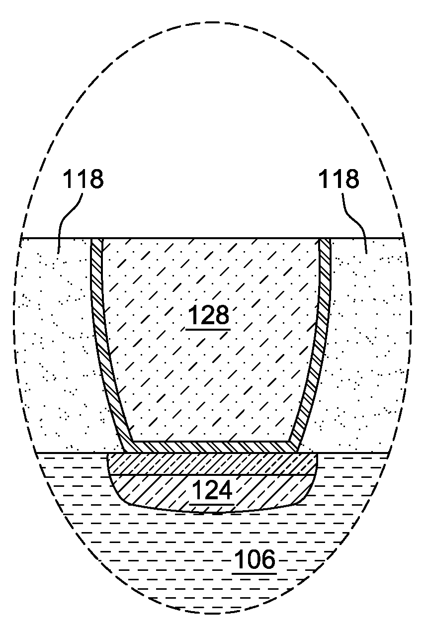
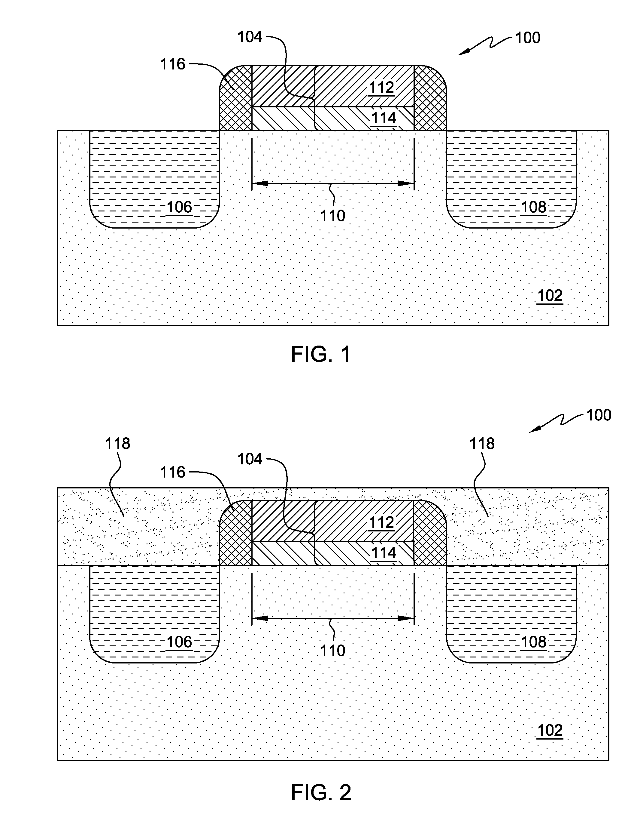
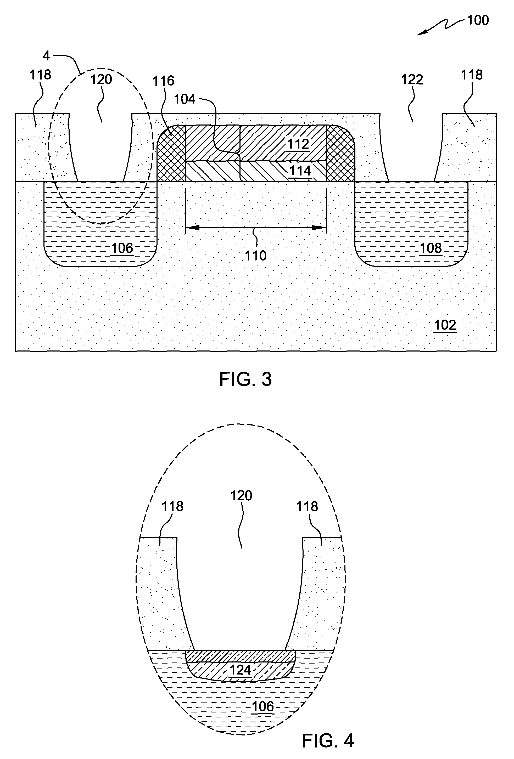
[0018]Detailed embodiments of the claimed structures and methods are disclosed herein; however, it is to be understood that the disclosed embodiments are merely illustrative of the claimed structures and methods that may be embodied in various forms. In addition, each of the examples given in connection with the various embodiments is intended to be illustrative, and not restrictive. Further, the figures are not necessarily to scale, some features may be exaggerated to show details of particular components. Therefore, specific structural and functional details disclosed herein are not to be interpreted as limiting, but merely as a representative basis for teaching one skilled in the art to variously employ the methods and structures of the present disclosure.

[0019]References in the specification to “one embodiment”, “an embodiment”, “an example embodiment”, etc., indicate that the embodiment described may include a particular feature, structure, or characteristic, but every embodime...


PUM

PropertyMeasurementUnit
widthaaaaaaaaaa
temperatureaaaaaaaaaa

Abstract

An electrical structure comprises a dielectric layer present on a semiconductor substrate. A contact opening is present through the dielectric layer. A nickel-tungsten alloy silicide is formed over the semiconductor substrate within the contact opening. A tungsten-containing nucleation layer formed within the contact opening covers the nickel-tungsten alloy silicide and at least a portion of a sidewall of the contact opening. A tungsten contact is formed within the contact opening and separated from the nickel-tungsten alloy silicide and at least a portion of the sidewall by the tungsten-containing nucleation layer.

Description

[0001]This application is a divisional of application Ser. No. 13 / 299,573 filed on Nov. 18, 2011, now pending.FIELD OF THE INVENTION[0002]This disclosure relates generally to semiconductor devices and more specifically to the formation of tungsten contacts for electrical connection to semiconductor devices.BACKGROUND OF THE INVENTION[0003]The fabrication of semiconductor devices involves forming electronic components in and on semiconductor substrates, such as silicon wafers. These electronic components may include one or more conductive layers, one or more insulation layers, and doped regions formed by implanting various dopants into portions of a semiconductor substrate to achieve specific electrical properties. Semiconductor devices include transistors, resistors, capacitors, and the like, with intermediate and overlying metallization patterns at varying levels, separated by dielectric materials, which interconnect the semiconductor devices to form integrated circuits.[0004]Field...

Claims


Application Information

Patent Timeline
Patent Type & Authority Patents(United States)
IPC IPC(8): H01L23/48
CPCH01L23/53261H01L21/28518H01L21/28556H01L23/485H01L23/53266H01L21/76876H01L21/76877H01L21/76814H01L2924/0002H01L2924/00
Inventor LAVOIE, CHRISTIANOZCAN, AHMET S.PAPADATOS, FILIPPOS
Owner GLOBALFOUNDRIES U S INC
Features
  • Generate Ideas
  • Intellectual Property
  • Life Sciences
  • Materials
  • Tech Scout
  • Unparalleled Data Quality
  • Higher Quality Content
  • 60% Fewer Hallucinations
Learn More