Check patentability & draft patents in minutes with Patsnap Eureka AI!

Electronic device and manufacturing method

a manufacturing method and electronic device technology, applied in the direction of semiconductor/solid-state device testing/measurement, transistors, basic electric elements, etc., can solve the problems of signal processing circuit characteristics that can deviate from the prescribed characteristics,

Active Publication Date: 2013-12-24
ADVANTEST CORP
View PDF52 Cites 1 Cited by
  • Summary
  • Abstract
  • Description
  • Claims
  • Application Information

AI Technical Summary

Benefits of technology

The solution enables the precise adjustment of electric characteristics in signal processing circuits, ensuring that the output signals meet prescribed specifications by using electron beam irradiation to correct any errors in the manufacturing process, thereby improving the reliability and accuracy of signal processing.

Problems solved by technology

However, due to variations in the manufacturing of the signal processing circuits, the characteristics thereof can deviate from the prescribed characteristics.
For example, etching variation of impurity density variation occurring in the process for forming the semiconductor circuits can cause an error in the characteristics of the signal processing circuits.

Method used


Image

  • Electronic device and manufacturing method
  • Electronic device and manufacturing method
  • Electronic device and manufacturing method

Examples


Embodiment Construction

[0018]Hereinafter, some embodiments of the present invention will be described. The embodiments do not limit the invention according to the claims, and all the combinations of the features described in the embodiments are not necessarily essential to means provided by aspects of the invention.

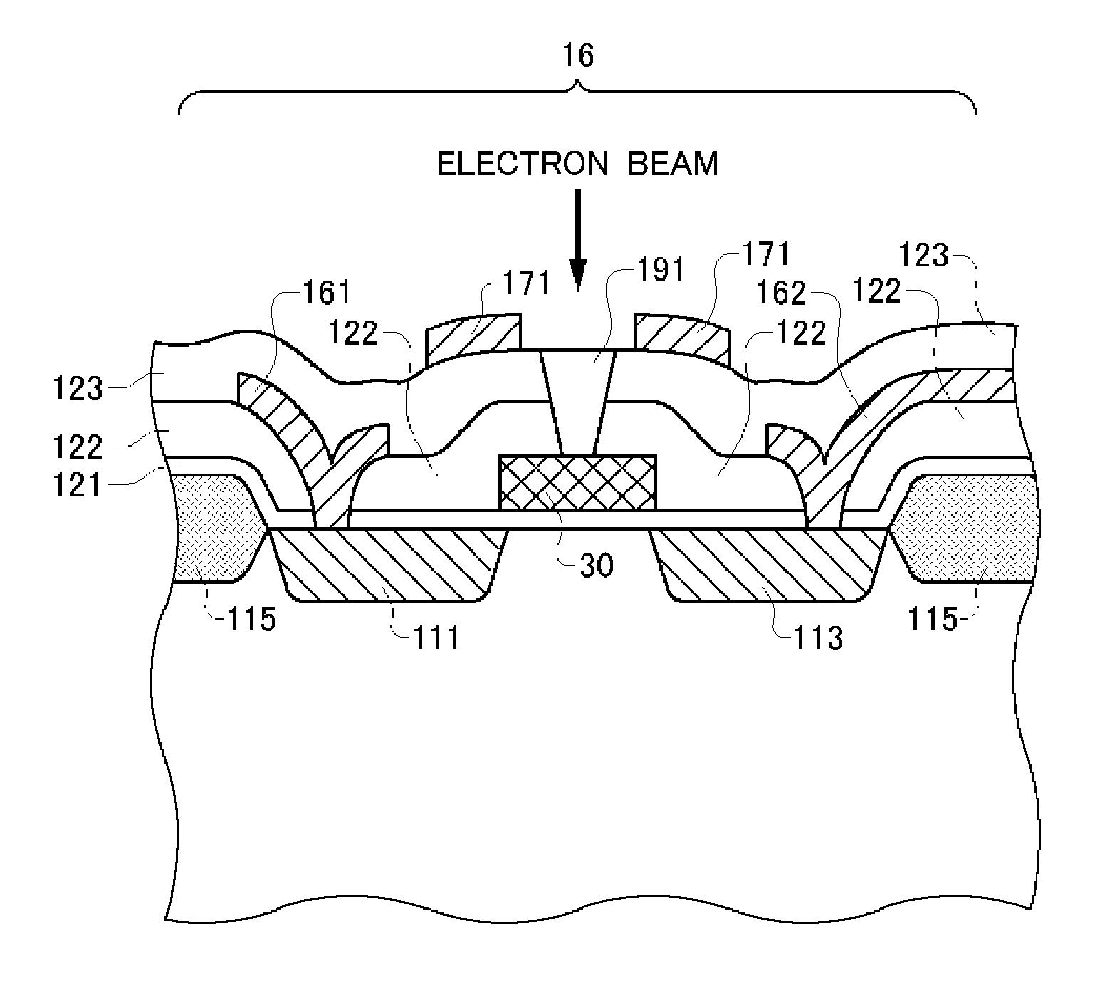
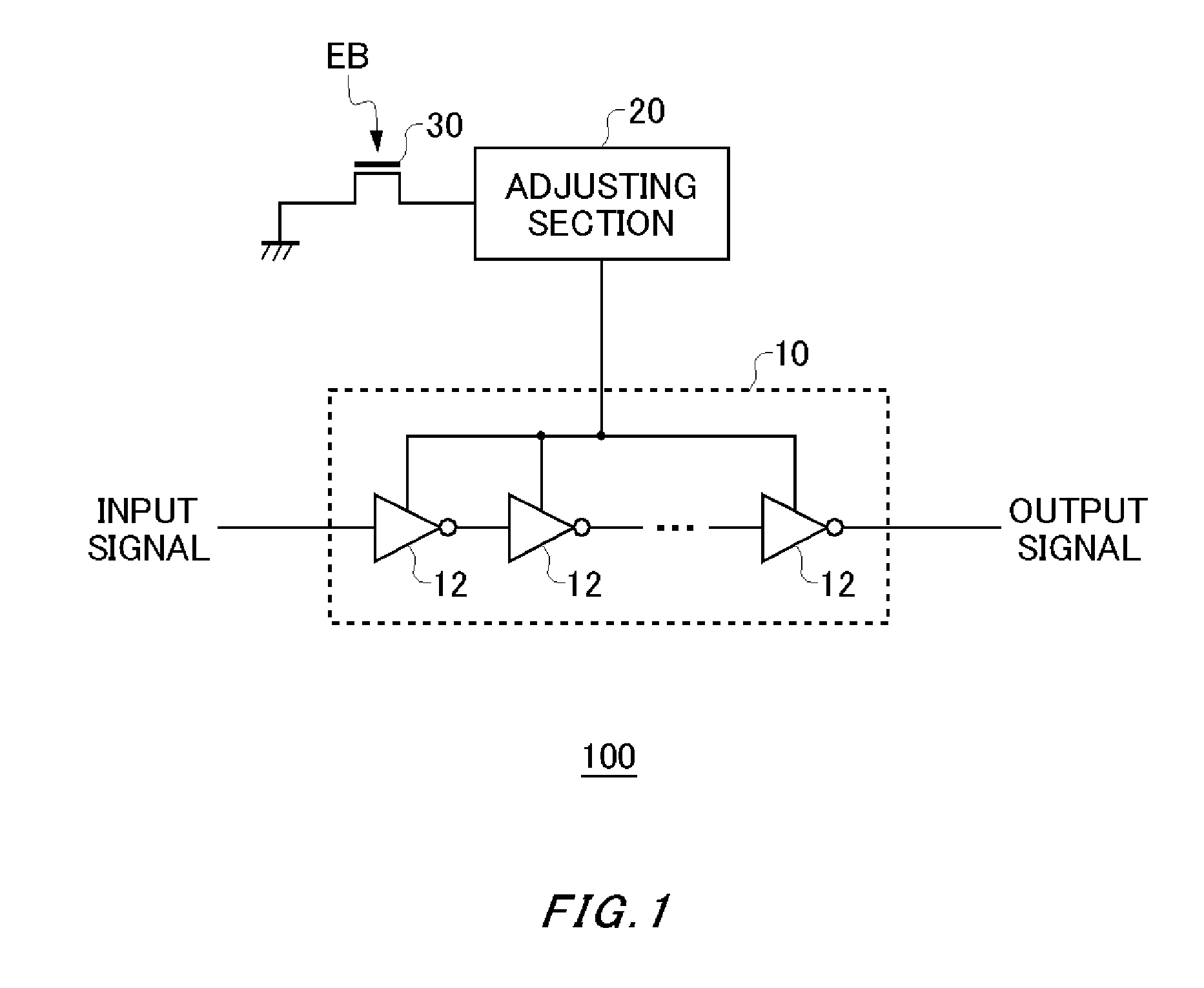
[0019]FIG. 1 shows an exemplary configuration of an electronic device 100 according to an embodiment of the present invention. The electronic device 100 generates an output signal by applying prescribed signal processing to an input signal. The electronic device 100 of the present embodiment includes a signal processing section 10, an adjusting section 20, and a floating electrode 30. The electronic device 100 may be a semiconductor circuit formed on a semiconductor substrate.

[0020]The signal processing section 10 receives the input signal and generates the output signal by applying the prescribed signal processing to the input signal. As shown in FIG. 1, the signal processing section 10 may be...


PUM


Abstract

Provided is an electronic device that generates an output signal corresponding to an input signal, comprising a signal processing section that receives the input signal and outputs the output signal corresponding to the input signal, and a floating electrode that accumulates a charge by being irradiated by an electron beam. The signal processing section adjusts electric characteristics of the output signal according to a charge amount accumulated in the floating electrode, and includes a transistor formed on the semiconductor substrate between an input terminal that receives the input signal and an output terminal that outputs the output signal. The floating electrode is formed between a gate electrode of the transistor and the semiconductor substrate.

Description

BACKGROUND[0001]1. Technical Field[0002]The present invention relates to an electronic device and a manufacturing method.[0003]2. Related Art[0004]An electronic device such as a semiconductor circuit includes a circuit that performs prescribed signal processing on an input signal. For example, an electronic device may include a circuit that delays the input signal or a circuit that changes the amplitude of the input signal. These signal processing circuits are formed to have prescribed characteristics, as shown in Patent Document 1, for example.[0005]Patent Document 1: Japanese Patent Application Publication No. 2001-7660[0006]However, due to variations in the manufacturing of the signal processing circuits, the characteristics thereof can deviate from the prescribed characteristics. For example, etching variation of impurity density variation occurring in the process for forming the semiconductor circuits can cause an error in the characteristics of the signal processing circuits.S...

Claims


Application Information

Patent Timeline
Patent Type & Authority Patents(United States)
IPC IPC(8): H01L29/66
CPCH01L21/28273H01L22/14H01L22/20H01L29/788H03K5/13H01L29/40114G01R31/305
Inventor WATANABE, DAISUKEOKAYASU, TOSHIYUKI
Owner ADVANTEST CORP
Features
  • R&D
  • Intellectual Property
  • Life Sciences
  • Materials
  • Tech Scout
  • Unparalleled Data Quality
  • Higher Quality Content
  • 60% Fewer Hallucinations
Learn More