Supercharge Your Innovation With Domain-Expert AI Agents!

Method of producing silicon carbide

a technology of silicon carbide and carbide, which is applied in the field of silicon carbide production, can solve the problems of vapor phase, low purity, contamination of wafers, etc., and achieve the effect of high productivity and comparative ease of production

Inactive Publication Date: 2013-12-31
NAT INST FOR MATERIALS SCI
View PDF28 Cites 0 Cited by
  • Summary
  • Abstract
  • Description
  • Claims
  • Application Information

AI Technical Summary

Benefits of technology

This method enables the simple and efficient production of high-purity silicon carbide with desired shape and dimensions, addressing the limitations of existing technologies by achieving high purity and productivity.

Problems solved by technology

If the silicon carbide material used in these steps comprises impurity elements, then these impurity elements may become incorporated within the wafer during heating of the wafer, causing contamination of the wafer.
However, silicon carbide produced using the Acheson process tends to suffer from low purity, silica reduction methods suffer from problems of uniformity resulting from heterogeneous mixing of the silica powder and the silicon carbide powder, and vapor phase methods suffer from problems of low productivity.
Recently, a method that uses a silicon metal alloy as the starting raw material has been reported (see Patent Document 1), and although this method enables silicon carbide to be obtained at low temperatures, the steps are complex, including conducting reaction under high pressure.
Further, methods of generating carbon-silicon bonds by mixing an ethyl silicate containing no carbon-silicon bonds with an organic compound, and then heating and reacting the mixture have also been reported (see Patent Documents 2 and 3), but the large quantity of decomposition products generated means it is difficult to claim that these methods offer a high degree of productivity.
Furthermore, because silicon carbide is usually resistant to sintering, conventionally, obtaining a silicon carbide molded item having a desired shape and dimensions is far from simple.[Patent Document 1] US 2006 / 0171873 A1[Patent Document 2] JP 11-171647 A[Patent Document 3] JP 2006-256937 A

Method used


Image

  • Method of producing silicon carbide
  • Method of producing silicon carbide
  • Method of producing silicon carbide

Examples


example 1

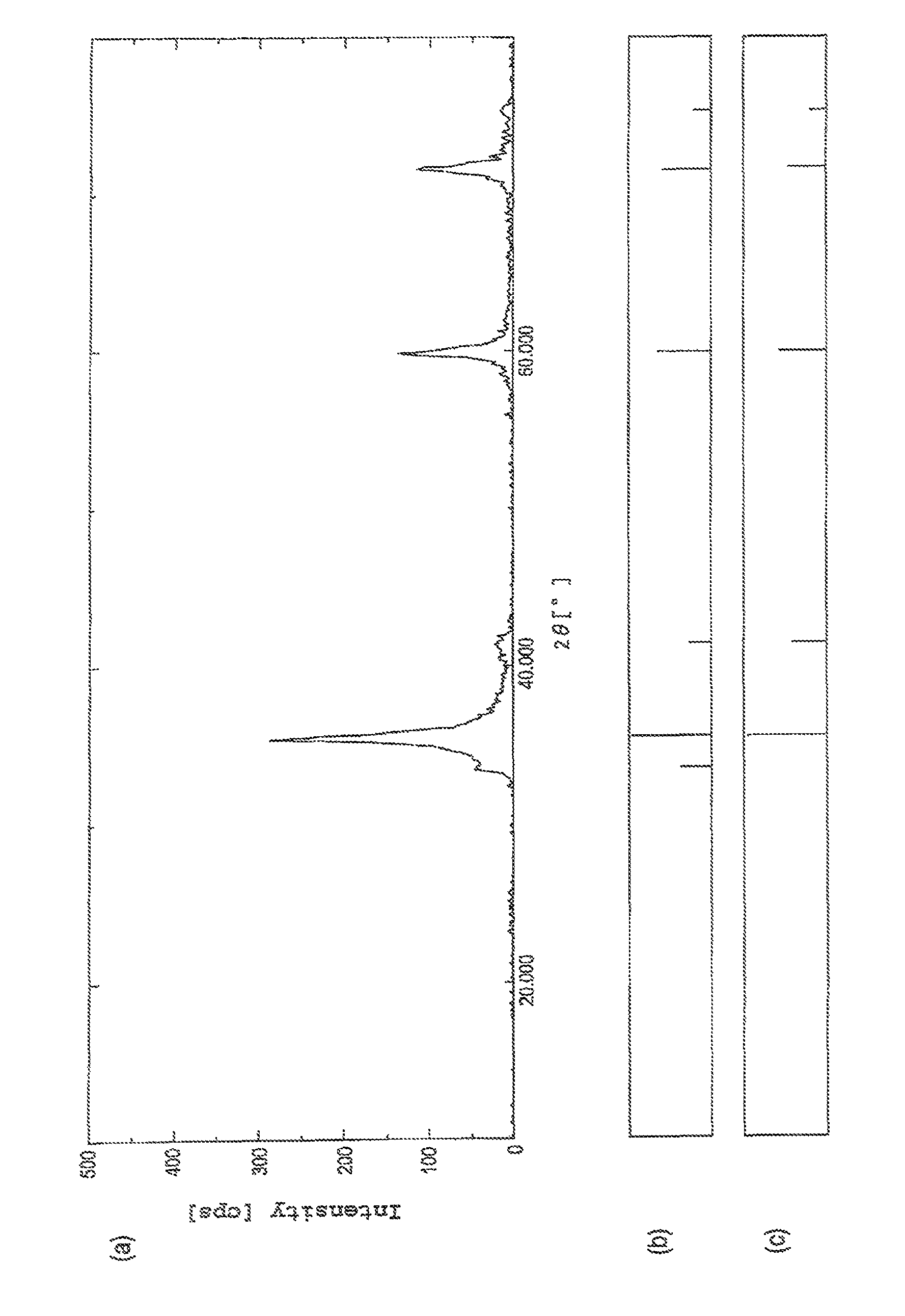
[0090]The components (A) and (B) described below were used as silicone components, and the component (C) described below was used as a platinum group metal-based catalyst. The quantity of each component is also shown below.

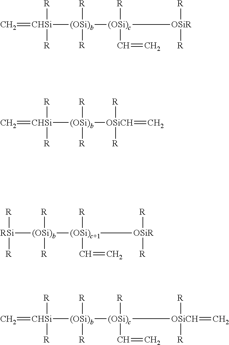
(A) 55 parts by mass of a diorganopolysiloxane containing alkenyl groups bonded to silicon atoms, represented by an average composition formula (5) shown below.

[0091]

(B) 45 parts by mass of a diorganopolysiloxane containing hydrogen atoms bonded to silicon atoms, represented by an average composition formula (6) shown below (wherein, the quantity of SiH groups within the component (B) per 1.0 mols of silicon atom-bonded alkenyl groups within the component (A) is 1.0 mols).

[0092]

(wherein, the molar ratio of SiH groups relative to all the silicon atoms within the molecule is 0.625).

(C) a toluene solution of a platinum-divinyltetramethyldisiloxane complex (platinum element content: 0.5% by mass), in a quantity equivalent to 50 ppm of the platinum element relative to ...

example 2

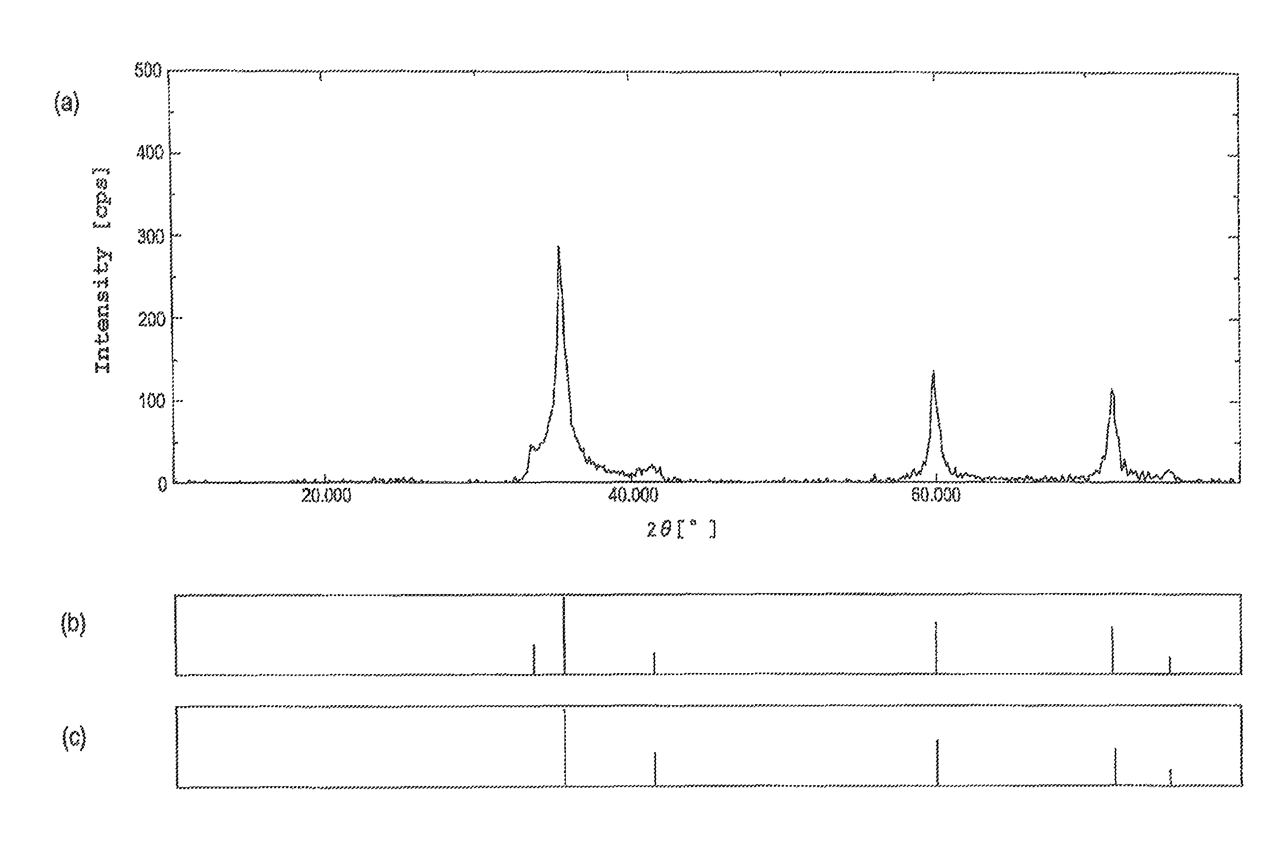
[0095]100 parts by mass of a silicone resin containing only MeSiO3 / 2 units as the siloxane units and also containing 5% by mass of hydroxyl groups (molecular weight: 1,000, average composition formula: Me(OH)0.2SiO1.3, softening point: 65° C.) was placed in an aluminum Petri dish and cured by heating at 200° C. for one hour. The resulting silicone cured product was subjected to a heat treatment in the same manner as Example 1, yielding a yellow-green solid. Analysis of this yellow-green solid in the same manner as that described in Example 1 revealed a carbon mass ratio of 30.4% by mass, an oxygen mass ratio of not more than 0.2% by mass, and an elemental ratio of SiC1.02.

example 3

[0096]The components (A) to (C) used in Example 1 and a component (D) described below as a silicon carbide powder were used in the respective quantities listed below.

(A) 55 parts by mass of the diorganopolysiloxane containing alkenyl groups bonded to silicon atoms and represented by the average composition formula (5) shown above.

(B) 45 parts by mass of the diorganopolysiloxane containing hydrogen atoms bonded to silicon atoms and represented by the average composition formula (6) shown above.

(C) a toluene solution of a platinum-divinyltetramethyldisiloxane complex (platinum element content: 0.5% by mass), in a quantity equivalent to 0.15% by mass relative to the combined mass of the component (A) and the component (B).

[0097](D) 327 parts by mass of a silicon carbide powder (volume average particle size: 10 μm) obtained by pulverizing the yellow-green solid of Example 1 using a ball mill (this quantity is equivalent to the quantity required to ensure that the silicon carbide powder ...


PUM

PropertyMeasurementUnit
ambient temperatureaaaaaaaaaa
average particle sizeaaaaaaaaaa

Abstract

A method of producing silicon carbide is provided. The method includes heating a cured product of a curable silicone composition in a non-oxidizing atmosphere at a temperature exceeding 1,500° C. but not more than 2,600° C. The method is capable of producing high-purity silicon carbide simply and at a high degree of productivity, and is capable of simply producing a silicon carbide molded item having a desired shape and dimensions.

Description

[0001]This application is a Divisional of co-pending application Ser. No. 12 / 340,084, filed on Dec. 19, 2008 for which priority is claimed under 35 U.S.C. §120 and under 35 U.S.C. §119(a) to Patent Application No. 2007-338066 filed in Japan, file Dec. 27, 2007. The entire contents of all of the above applications are hereby incorporated by reference.BACKGROUND OF THE INVENTION[0002]1. Field of the Invention[0003]The present invention relates to a method of producing silicon carbide that is capable of producing high-purity silicon carbide simply and at a high degree of productivity using a silicone composition.[0004]2. Description of the Prior Art[0005]Silicon carbide ceramics are chemically stable at both normal temperatures and high temperatures, and exhibit excellent mechanical strength at high temperature, and are therefore widely used as high-temperature materials. In recent years, in the field of semiconductor production, high-purity silicon carbide ceramic sintered bodies, whi...

Claims


Application Information

Patent Timeline
Patent Type & Authority Patents(United States)
IPC IPC(8): C01B31/36C01B32/942
CPCC04B2235/3289C04B2235/483C04B2235/79C04B35/565C04B35/571C04B2235/5436C04B2235/3826C04B2235/723C04B2235/602C04B35/6325C01B31/36C04B2235/9661C04B35/6269C01B32/977C01B32/956
Inventor TANAKA, HIDEHIKOAOKI, YOSHITAKA
Owner NAT INST FOR MATERIALS SCI
Features
  • R&D
  • Intellectual Property
  • Life Sciences
  • Materials
  • Tech Scout
  • Unparalleled Data Quality
  • Higher Quality Content
  • 60% Fewer Hallucinations
Learn More