Check patentability & draft patents in minutes with Patsnap Eureka AI!

Semiconductor memory apparatus

a memory device and semiconductor technology, applied in the field of semiconductor memory devices, can solve the problems of reducing the threshold voltage, limiting the reduction of the threshold voltage, and deteriorating the low voltage characteristi

Active Publication Date: 2014-04-15
SK HYNIX INC
View PDF7 Cites 0 Cited by
  • Summary
  • Abstract
  • Description
  • Claims
  • Application Information

AI Technical Summary

Benefits of technology

This configuration allows for improved low voltage characteristics while maintaining reduced leakage currents, enabling faster data output and efficient sensing operations without compromising the voltage levels.

Problems solved by technology

However, in the above-described known bit line sense amplifier, a low voltage characteristic may be deteriorated due to a high threshold voltage of a MOS transistor forming the bit line sense amplifier.
Furthermore, if the threshold voltage is reduced so as to improve the low voltage characteristic, a leakage current may increase.
Therefore, there is a limit in reducing the threshold voltage.

Method used


Image

  • Semiconductor memory apparatus
  • Semiconductor memory apparatus
  • Semiconductor memory apparatus

Examples


Embodiment Construction

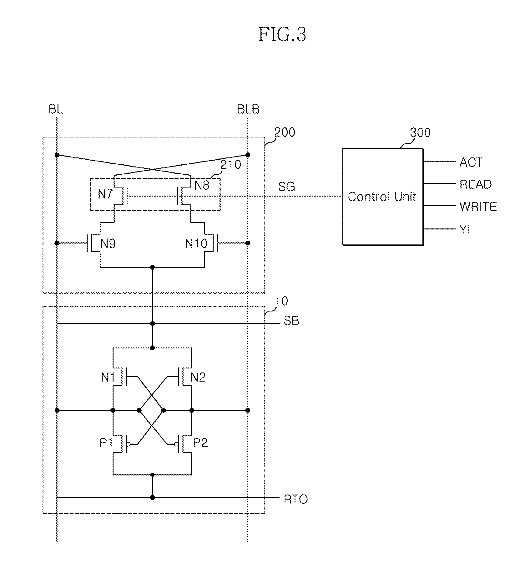
[0036]Hereinafter, a semiconductor memory apparatus according to the present invention will be described below with reference to the accompanying drawings through exemplary embodiments.

[0037]FIG. 3 is a configuration diagram illustrating a semiconductor memory apparatus including a bit line sense amplifier according to an embodiment of the present invention.

[0038]The semiconductor memory apparatus of FIG. 3 includes bit line sense amplifiers 10 and 200 and a controller 300 configured to generate a switching signal SG for controlling the bit line sense amplifiers.

[0039]The bit line sense amplifiers 10 and 200 include a first sense amplification unit 10 and a second sense amplification unit 200.

[0040]The first sense amplification unit 10 may include the known sense amplifier illustrated in FIG. 1, and may have the same configuration and operation as described above.

[0041]The second sense amplification unit 200 includes a transistor pair, e.g., ninth and tenth NMOS transistors N9 and N...


PUM


Abstract

A semiconductor memory apparatus includes: a first sense amplification unit including first and second inverters configured to be driven to voltage levels of a power driving signal and a ground driving signal and forming a latch structure between a bit line and a bit line bar; and a second sense amplification unit including first and second transistors configured to be driven to the voltage level of the ground driving signal and forming a latch structure between the bit line and the bit line bar when an activated switching signal is applied, wherein a threshold voltage of the second sense amplification unit is set lower than that of the first sense amplification unit.

Description

CROSS-REFERENCES TO RELATED APPLICATION[0001]The present application claims priority under 35 U.S.C. §119(a) to Korean application number 10-2011-0135694 filed on Dec. 15, 2011, in the Korean Intellectual Property Office, which is incorporated herein by reference.BACKGROUND[0002]1. Technical Field[0003]The present invention relates generally to a semiconductor memory apparatus, and more particularly to a semiconductor memory apparatus including a bit line sense amplifier.[0004]2. Related Art[0005]A bit line sense amplifier used in a semiconductor memory apparatus senses and amplifies data stored in a memory cell. The bit line sense amplifier is coupled to a bit line pair including a bit line BL connected to the memory cell, and amplifies the voltage level of data detected from the bit line BL with which the charge of memory cell is shared.[0006]FIG. 1 illustrates a known bit line sense amplifier. Referring to FIG. 1, the bit line sense amplifier includes two pairs of inverters N1, P...

Claims


Application Information

Patent Timeline
Patent Type & Authority Patents(United States)
IPC IPC(8): G11C7/06
CPCG11C29/12G11C7/08G11C7/12G11C7/065G11C2029/1204G11C7/06
Inventor LIM, KYU NAMJANG, WOONG JU
Owner SK HYNIX INC
Features
  • R&D
  • Intellectual Property
  • Life Sciences
  • Materials
  • Tech Scout
  • Unparalleled Data Quality
  • Higher Quality Content
  • 60% Fewer Hallucinations
Learn More