Supercharge Your Innovation With Domain-Expert AI Agents!

Clock distribution circuit

a clock distribution and circuit technology, applied in the direction of generating/distributing signals, instruments, pulse techniques, etc., can solve the problems of inability to adjust the clock phase accurately, the design constraints of including a greater timing margin, and the difference in electrical properties, etc., to achieve the effect of high accuracy of clock phase adjustments

Active Publication Date: 2014-04-29
CANON KK
View PDF3 Cites 1 Cited by
  • Summary
  • Abstract
  • Description
  • Claims
  • Application Information

AI Technical Summary

Benefits of technology

This approach results in a clock distribution circuit that effectively suppresses feedback path discrepancies, ensuring accurate phase adjustments and reducing the impact of manufacturing-induced delays, thereby improving the precision of clock phase synchronization.

Problems solved by technology

That is, since these factors of discrepancies influence the design values of timing, design constraints must be added of including greater timing margins.
In particular, differences in electrical properties are a direct adverse factor of clock skew, and in locations such as interfaces between blocks having long distances from the clock branch, timing margins as countermeasures of discrepancies applied to route differences use an undesirably large portion of the timing in the cycle time.
However, there is a probability that phase adjustments will be insufficient if routes to sequential circuits of terminals driven by the clock are designed independently.
However, there are currently further advances being made in miniaturization and it is necessary to give consideration at the design stage up to problems of discrepancies occurring in manufacturing processes such as exposure of mask patterns and the forming and polishing of thin films that constitute elements and wiring.
That is, even if circuits are laid out using exactly the same structure of elements and wiring, discrepancies in the manufacturing processes cannot be ignored in which shapes and electrical properties change undesirably at the manufacturing stage due to the positions of placement and the patterns of peripheral circuits.
Since systematic factors and random factors are both related in the influence of discrepancies occurring in manufacturing processes, it is difficult to accurately estimate these at the design stage.
However, in processes where greater miniaturization is implemented, the influence of discrepancies that occur between the clock drivers and the wiring within independent routes after the feedback path branch cannot be ignored.
Accordingly, it is difficult with conventional techniques to eliminate completely problems of discrepancies, and reduced precision in phase adjustments is anticipated.

Method used


Image

  • Clock distribution circuit
  • Clock distribution circuit
  • Clock distribution circuit

Examples


embodiment 1

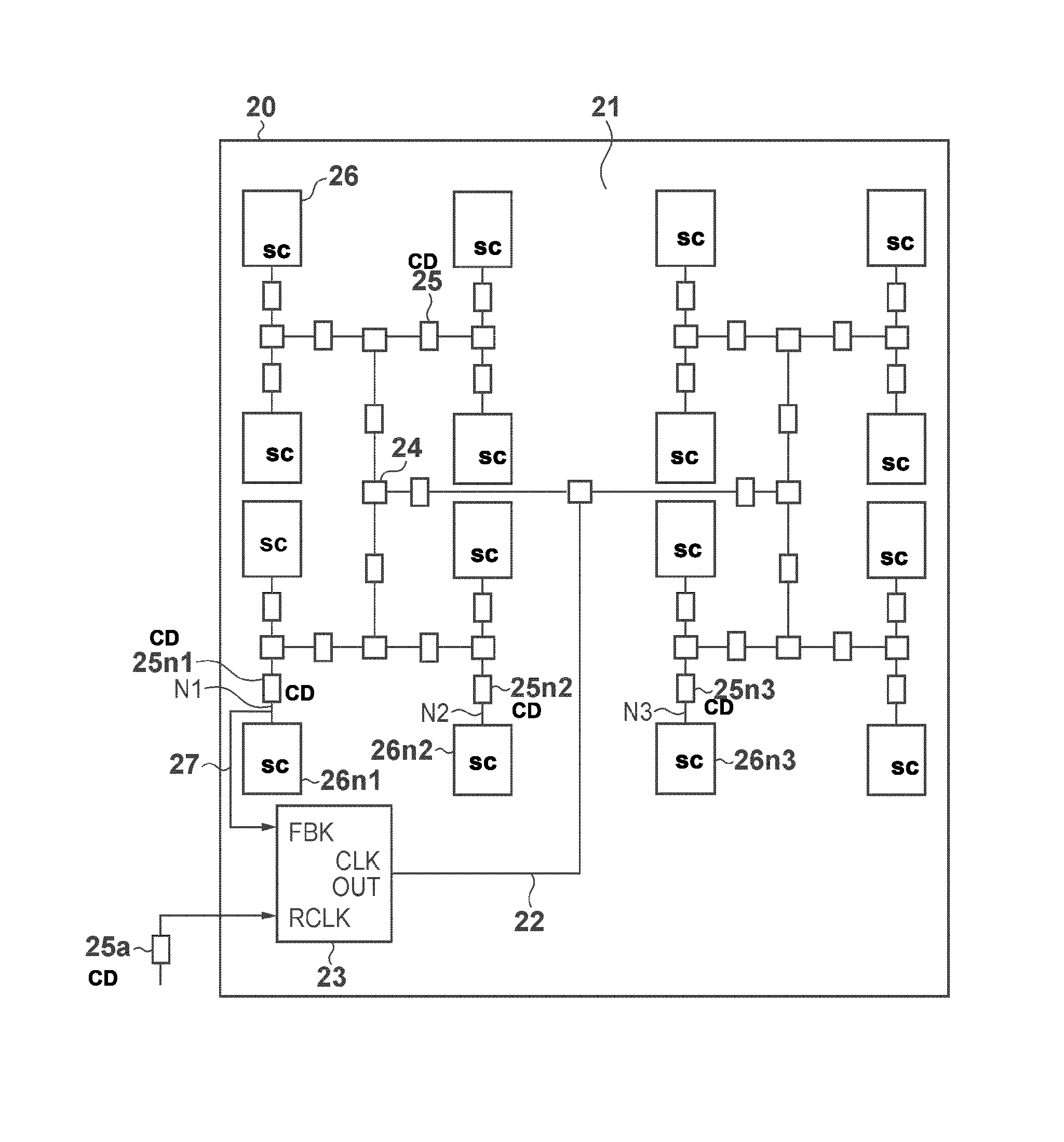
[0032]Hereinafter, description is given regarding a clock distribution circuit according to an embodiment (the abbreviations used in FIG. 1 are also used in FIGS. 3 and 5). FIG. 3 is a schematic block diagram showing one example of a configuration of a clock distribution circuit according to the present embodiment. A clock distribution circuit 21 is provided on a semiconductor integrated circuit and distributes a clock signal, which is generated as a reference signal of a frequency and phase of an external clock signal, to multiple sequential circuits 26. The sequential circuits 26 operate based on the supplied clock signal.

[0033]The clock distribution circuit 21 is provided with a clock distribution network 22, a clock generation circuit 23 such as a PLL or a DLL, a distribution circuit 24, a clock driver 25, and wiring. Of final stage clock drivers of the clock distribution network, a branch point N1 is provided at a clock driver near the clock generation circuit 23 as a feedback ...

embodiment 2

[0048]In the foregoing embodiment 1, the branch point N1 of the feedback path was obtained from the output terminal of the preceding stage clock driver 25n1 of the sequential circuit near the clock generation circuit 23. However, in a case where concentration of wiring is occurring near the clock generation circuit 23, the branch point may be provided so that wire congestion does not occur. For example, consider a case where a circuit having multitudinous connection relationships with SRAM or with another block, or a circuit that generates a control signal is present near the clock generation circuit. When the clock driver branch point is determined so as to avoid a concentration of wiring, phase adjustments can be performed so that wire congestion does not occur. Other than this, this is the same as embodiment 1.

embodiment 3

[0049]In embodiment 3, the branch point is provided at an output terminal of a preceding stage clock driver of a sequential circuit having low relevance to at least one of function and performance, that is, having a data path in which there is leeway in the timing design, or a sequential circuit having data path in which there is a large timing margin.

[0050]As in embodiment 1, there are two methods of setting the feedback path. One is a method of selecting the feedback path branch point by extracting a path in which there is leeway in the timing design based on layout data after clock routing and after placement and routing. The other is a method of providing a feedback path by extracting in advance a data path in which there is leeway in the timing design, and controlling the placement of feedback path branch points by implementing placement restrictions with a floor plan, which is an outline placement process prior to executing placement and routing.

[0051]First, description is giv...


PUM


Abstract

A clock distribution circuit is provided with a clock generation circuit configured to generate a clock signal, a clock distribution network in which the clock signal is distributed, and a sequential circuit configured to operate on the clock signal distributed through a branch point of the clock distribution network. The clock distribution circuit is further provided with a clock generation circuit configured to input as a feedback signal the clock signal that has branched from the branch point and to output the clock signal to the clock distribution network based on the inputted feedback signal and a reference clock signal. The branch point is provided at a clock driver near the clock generation circuit, among preceding stage clock drivers of the sequential circuit of the clock distribution network.

Description

BACKGROUND OF THE INVENTION[0001]1. Field of the Invention[0002]The present invention relates to clock distribution circuits.[0003]2. Description of the Related Art[0004]Along with increasing miniaturization of semiconductor integrated circuits in recent years, problems of manufacturing discrepancies brought about by new factors that did not require consideration at the design stage are exerting a large influence on circuit designs in conventional semiconductor processes.[0005]In the processes of generations where miniaturization was not so far advanced, the statistical distribution of individual differences caused by lots, wafers, materials, and the like were generally handled as discrepancies. In the processes of advanced miniaturization of the 90 nm generations onward, in addition to the aforementioned individual differences, it has also become necessary to give consideration at the design stage to individual differences of transistors and wiring within a chip due to voltage drop...

Claims


Application Information

Patent Timeline
Patent Type & Authority Patents(United States)
IPC IPC(8): H03K3/00
CPCG06F1/10
Inventor FUJIMORI, KAZUYA
Owner CANON KK
Features
  • R&D
  • Intellectual Property
  • Life Sciences
  • Materials
  • Tech Scout
  • Unparalleled Data Quality
  • Higher Quality Content
  • 60% Fewer Hallucinations
Learn More