Pixel circuit driving method, light emitting device, and electronic apparatus
a technology of light emitting elements and driving transistors, applied in the direction of electric digital data processing, instruments, computing, etc., can solve the problems of inability to correct the variation of driving current, the electric characteristic variation of the driving transistor becomes an issue, and the deviation of the target value or the difference between elements
- Summary
- Abstract
- Description
- Claims
- Application Information
AI Technical Summary
Benefits of technology
Problems solved by technology
Method used
Image

Examples
first embodiment
B: First Embodiment
B-1: Configuration and Operation of Light Emitting Device
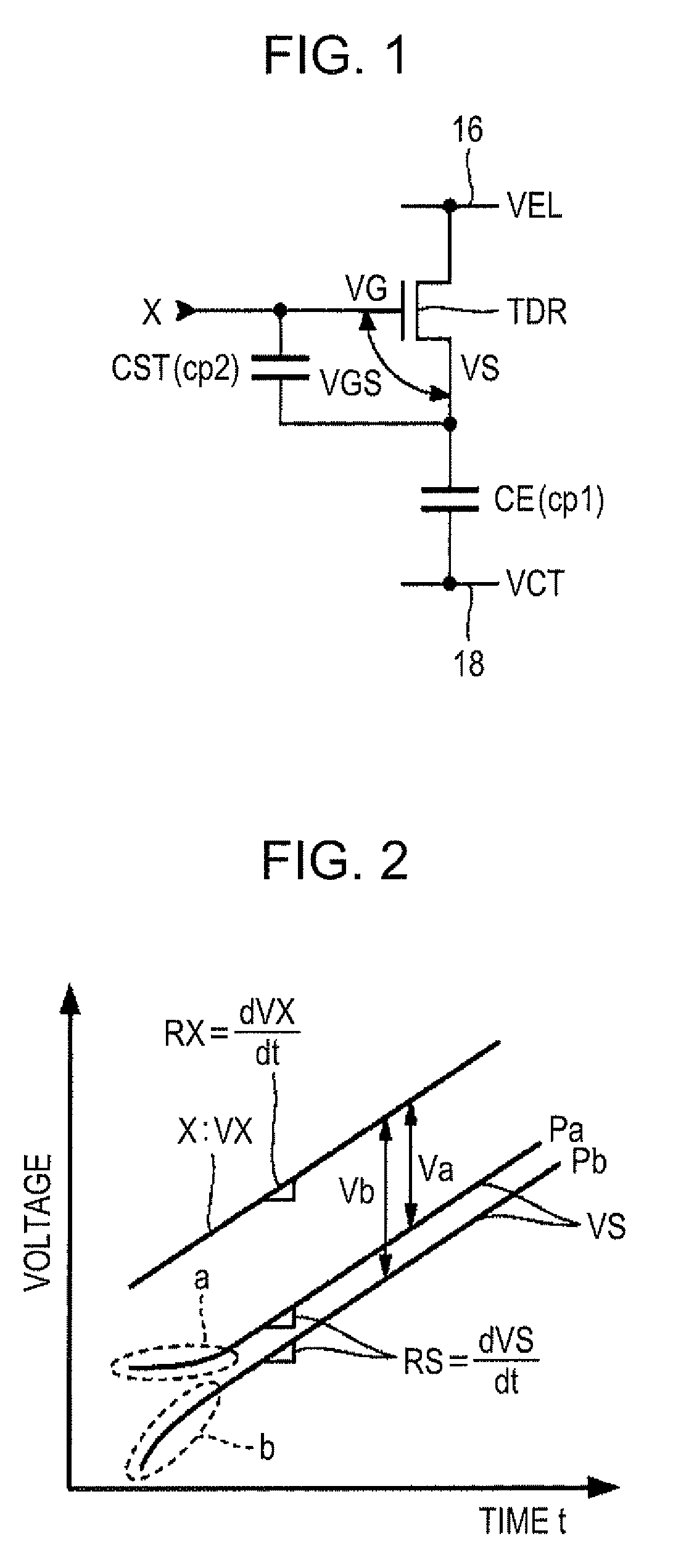
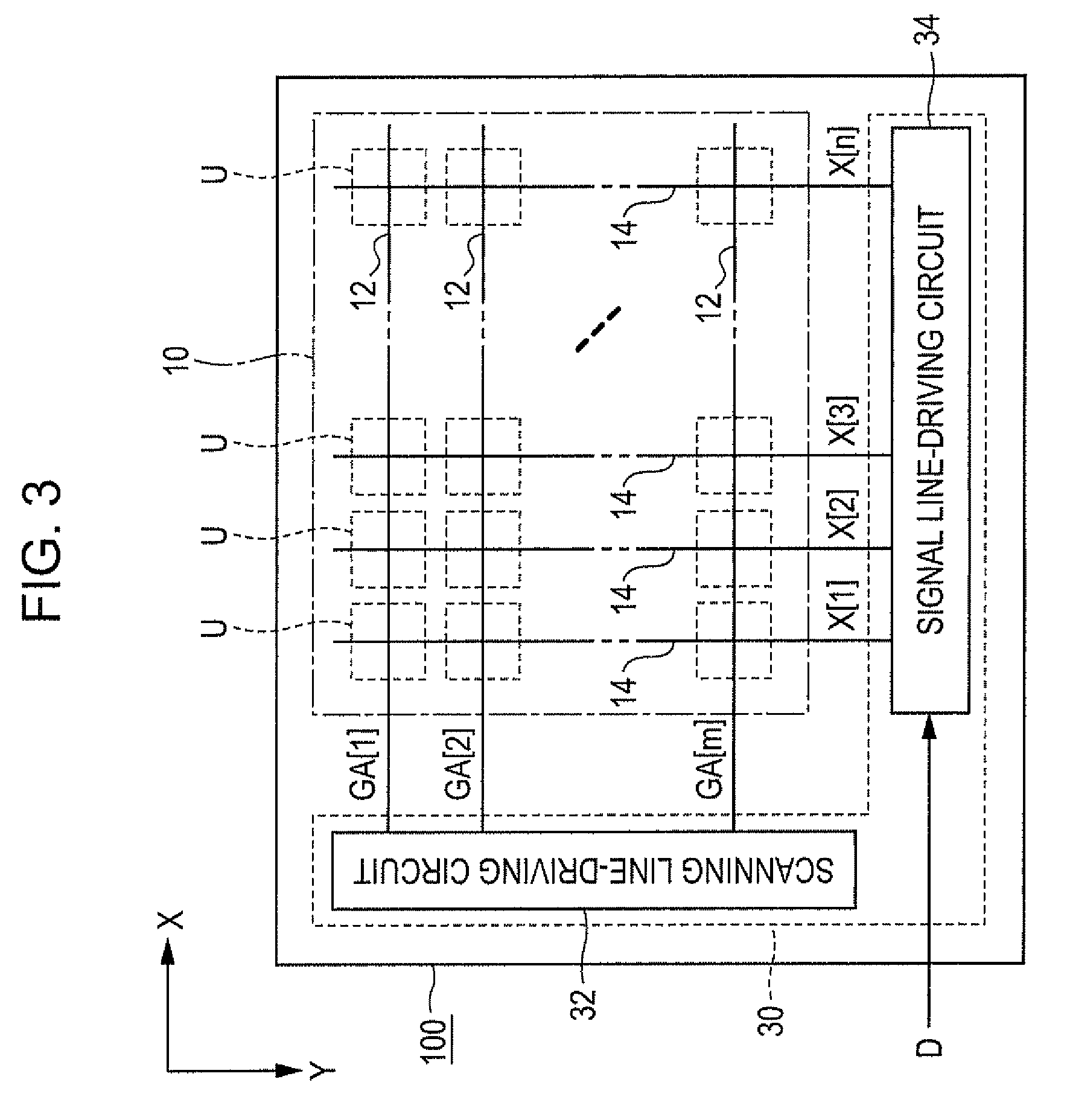
[0073]FIG. 3 is a block diagram of a light emitting device according to a first embodiment of the invention. The light emitting device 100 is mounted on an electronic apparatus as a display device displaying images. As illustrated in FIG. 3, the light emitting device 100 includes a device portion 10 on which a plurality of pixel circuits U is arranged, and a driving circuit 30 for driving the pixel circuits U. The driving circuit 30 is configured to include a scanning line-driving circuit 32 and a signal line-driving circuit 34. The driving circuit 30 is implemented on a plurality of distributed integrated circuits, for example. It should be noted that at least a part of the driving circuit 30 may be constructed of thin film transistors which are formed on a substrate, together with the pixel circuits U.
[0074]In the device portion 10, μ scanning lines 12 extending in the X direction and n signal lines 14 ext...
second embodiment
C-1: Second Embodiment
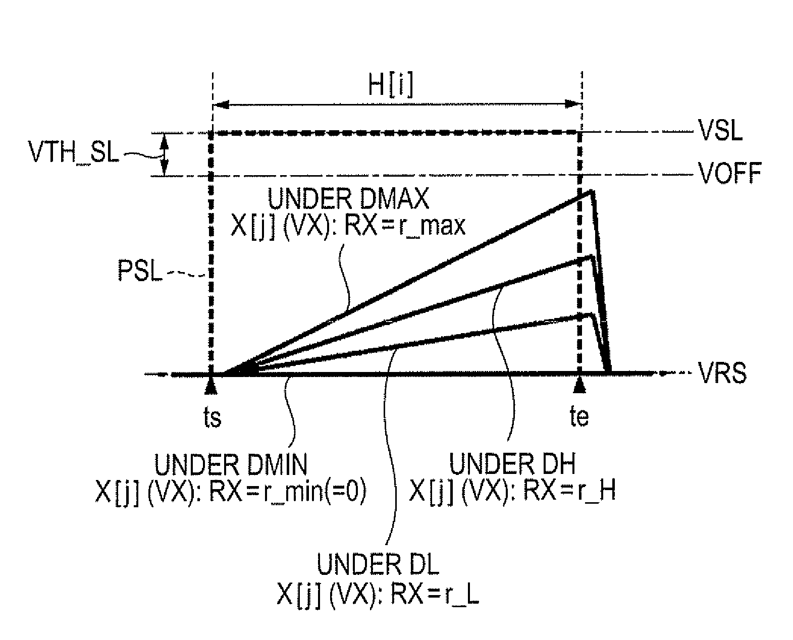
[0103]FIG. 12 is a waveform diagram of the driving signal X[j] in the unit time period H[i] according to the second embodiment of the invention. As illustrated in FIG. 12, when the minimum gradation DMIN or the intermediate gradation DL lower than a predetermined value is specified, similar to the case of the first embodiment, the waveform (time rate of change RX) of the driving signal X[j] is chosen so that the potential VX of the driving signal X[j] at the end point te of the unit time period H[i] is lower than a potential VOFF (a potential lower than the selection potential VSL by the amount of the threshold voltage VTH_SL of the select switch TSL). Therefore, when the minimum gradation DMIN or the intermediate gradation DL is specified, the select switch TSL is changed to the OFF state at the end point te (the trailing edge of the selection pulse PSL) of the unit time period H[i] so that the supply of the driving signal X[j] to the gate of the driving trans...
third embodiment
C-2: Third Embodiment
[0109]FIG. 13 is a waveform diagram of the driving signal X[j] in the unit time period H[i] according to the third embodiment of the invention. In the first and second embodiments, the case where the potential VX of the driving signal X[j] begins to change at the starting point ts of the unit time period H[i] was illustrated. However, in the present embodiment, as illustrated in FIG. 13, the potential VX of the driving signal X[j] begins to change from the reference potential VRS at a point in time after the passing of an adjustment time TA from the starting point ts (the leading edge of the selection pulse PSL) of the unit time period H[i].
[0110]The adjustment time TA is set to be variable in accordance with the specified gradation D. More specifically, the signal line-driving circuit 34 generates the driving signal X[j] so that the higher the specified gradation D, the longer the adjustment time TA becomes, as illustrated in FIG. 13. For example, the adjustmen...
PUM
 Abstract
Description
Claims
Application Information
 - R&D
- Intellectual Property
- Life Sciences
- Materials
- Tech Scout
- Unparalleled Data Quality
- Higher Quality Content
- 60% Fewer Hallucinations
Browse by: Latest US Patents, China's latest patents, Technical Efficacy Thesaurus, Application Domain, Technology Topic, Popular Technical Reports.
© 2025 PatSnap. All rights reserved.Legal|Privacy policy|Modern Slavery Act Transparency Statement|Sitemap|About US| Contact US: help@patsnap.com