Check patentability & draft patents in minutes with Patsnap Eureka AI!

Cu surface plasma treatment to improve gapfill window

a plasma treatment and gap filling technology, applied in the field of substrate processing methods, can solve the problems of increasing processing capabilities, increasing the difficulty of traditional deposition processes in filling nanometer-sized openings, and reducing the electrical conductivity of the conductive seed layer, so as to reduce the electrical conductivity of the seed layer

Inactive Publication Date: 2014-07-01
APPLIED MATERIALS INC
View PDF37 Cites 0 Cited by
  • Summary
  • Abstract
  • Description
  • Claims
  • Application Information

AI Technical Summary

Benefits of technology

This approach ensures void-free filling of nanometer-sized features by controlling the deposition rate, preventing overhangs and ensuring complete metal filling in high aspect ratio geometries, thereby enhancing the quality and density of semiconductor circuits.

Problems solved by technology

The shrinking dimensions of circuits and devices have placed additional demands on processing capabilities.
Many traditional deposition processes have difficulty filling nanometer-sized openings where the aspect ratio exceeds 4:1, and particularly where the aspect ratio exceeds 10:1.
Therefore, there is much effort directed at the formation of substantially void-free, nanometer-sized features having high aspect ratio geometries.

Method used


Image

  • Cu surface plasma treatment to improve gapfill window
  • Cu surface plasma treatment to improve gapfill window
  • Cu surface plasma treatment to improve gapfill window

Examples


Embodiment Construction

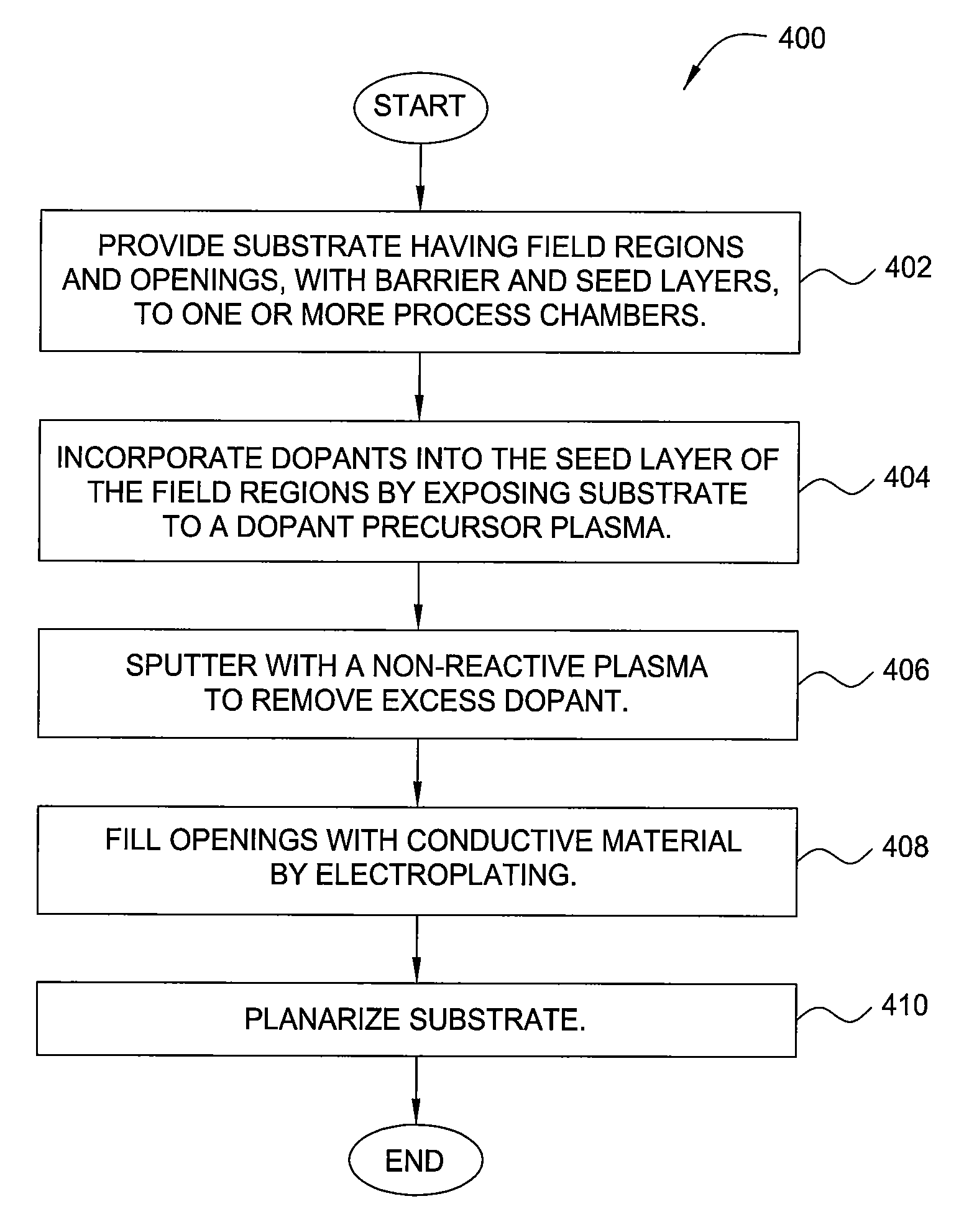
[0018]Embodiments of the invention generally provide methods for controlling deposition rate on a substrate in an electroplating process. A substrate having openings in field regions to be filled with metal is provided to one or more process chambers. The processes described herein may be performed in a single chamber, or in multiple chambers if desired and convenient. The substrate may be degassed, and the surface subjected to a cleaning process, prior to the plating process, if necessary. A barrier layer is deposited over the substrate surface, followed by a metal seed layer. The metal most commonly used for the seed layer and subsequent gap fill is copper (Cu), although other metals, such as aluminum, or alloys of metals may be used for gap fill or for the seed layer. Following deposition of the seed layer, the substrate surface is exposed to a plasma treatment using nitrogen gas, either substantially pure or mixed with a carrier gas such as argon or helium. Conditions of the pla...


PUM

PropertyMeasurementUnit
poweraaaaaaaaaa
poweraaaaaaaaaa
RF poweraaaaaaaaaa

Abstract

A method and apparatus for selectively controlling deposition rate of conductive material during an electroplating process. Dopants are predominantly incorporated into a conductive seed layer on field regions of a substrate prior to filling openings in the field regions by electroplating. A substrate is positioned in one or more processing chambers, and barrier and conductive seed layers formed. A dopant precursor is provided to the chamber and ionized, with or without voltage bias. The dopant predominantly incorporates into the conductive seed layer on the field regions. Electrical conductivity of the conductive seed layer on the field regions is reduced relative to that of the conductive seed layer in the openings, resulting in low initial deposition rate of metal on the field regions during electroplating, and little or no void formation in the metal deposited in the openings.

Description

CROSS-REFERENCE TO RELATED APPLICATIONS[0001]This application claims benefit of U.S. Provisional Patent Application Ser. No. 61 / 021,259, filed Jan. 15, 2008, which is herein incorporated by reference.BACKGROUND OF THE INVENTION[0002]1. Field of the Invention[0003]Embodiments of the invention relate generally to methods for processing a substrate during semiconductor manufacturing. Specifically, embodiments of the invention relate to methods of treating a conductive seed layer prior to an electrochemical deposition process.[0004]2. Description of the Related Art[0005]Reliably producing nanometer-sized features is one of the key technologies for the next generation of semiconductor devices. The shrinking dimensions of circuits and devices have placed additional demands on processing capabilities. The multilevel interconnects that lie at the heart of integrated circuit technology require precise processing of high aspect ratio features, such as vias and other interconnects. Reliable fo...

Claims


Application Information

Patent Timeline
Patent Type & Authority Patents(United States)
IPC IPC(8): C25D5/34C25D7/12
CPCH01L21/76864C25D21/12H01L21/76856H01L21/76877C25D5/02H01L21/76843H01L21/76862H01L21/76873
Inventor LUO, QIANSUNDARRAJAN, ARVINDCHUNG, HUATANG, XIANMINYU, JICK M.NARASIMHAN, MURALI K.
Owner APPLIED MATERIALS INC
Features
  • R&D
  • Intellectual Property
  • Life Sciences
  • Materials
  • Tech Scout
  • Unparalleled Data Quality
  • Higher Quality Content
  • 60% Fewer Hallucinations
Learn More