Check patentability & draft patents in minutes with Patsnap Eureka AI!

Method for manufacturing a diode, and a diode

a manufacturing method and diode technology, applied in the direction of semiconductor devices, semiconductor/solid-state device details, electrical apparatus, etc., can solve the problems of deterioration of the properties of the diode, and achieve the effects of preventing or clearly reducing the development of crystal disruption, improving the longevity of the diode, and producing in very few processing steps

Active Publication Date: 2014-12-02
ROBERT BOSCH GMBH
View PDF3 Cites 0 Cited by
  • Summary
  • Abstract
  • Description
  • Claims
  • Application Information

AI Technical Summary

Benefits of technology

[0006]The method according to the present invention for manufacturing a diode and the diode according to the present invention have the advantage that the chosen separation method prevents or clearly reduces the development of crystal disruptions in the area of the separation edges. It is therefore no longer necessary to perform subsequent processing steps to remove the crystal damage that has occurred. Both subsequent etching processes as well as subsequent temperature treatments may therefore be omitted. A high-quality diode is thus created, which may be produced in very few processing steps. Furthermore, a possible contamination by etching chemicals is fundamentally prevented, which improves the longevity of the diode.
[0007]It is particularly simple to perform local heating by a laser beam and local cooling by a gas jet or water jet. The disturbances, which are the starting point of the fissure propagation, may be produced in a particularly simple manner by scoring, sawing or a laser. It is particularly advantageous that there is no subsequent processing by an etching process since thus additional contaminations of the diode are eliminated and the extra expenditure for such an etching process is not required.

Problems solved by technology

Such a sawing process produces crystal defects in the area of the cut edges, which result in a deterioration of the properties of the diodes developed in this manner.

Method used


Image

  • Method for manufacturing a diode, and a diode
  • Method for manufacturing a diode, and a diode
  • Method for manufacturing a diode, and a diode

Examples


Embodiment Construction

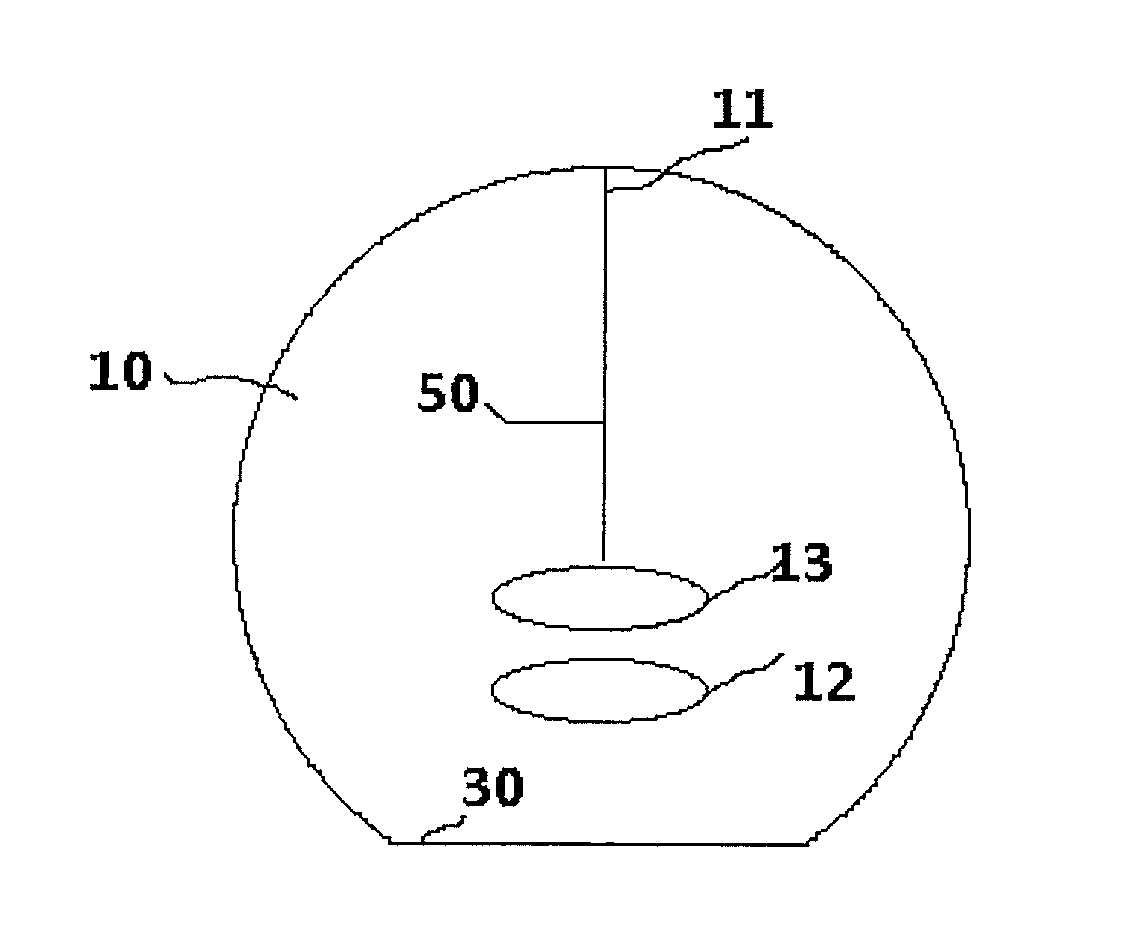
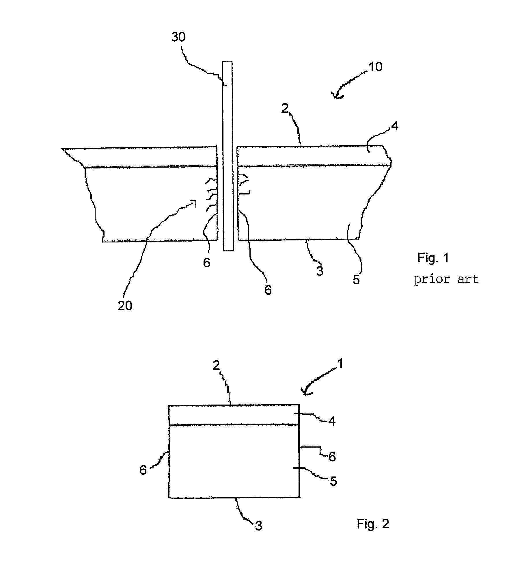
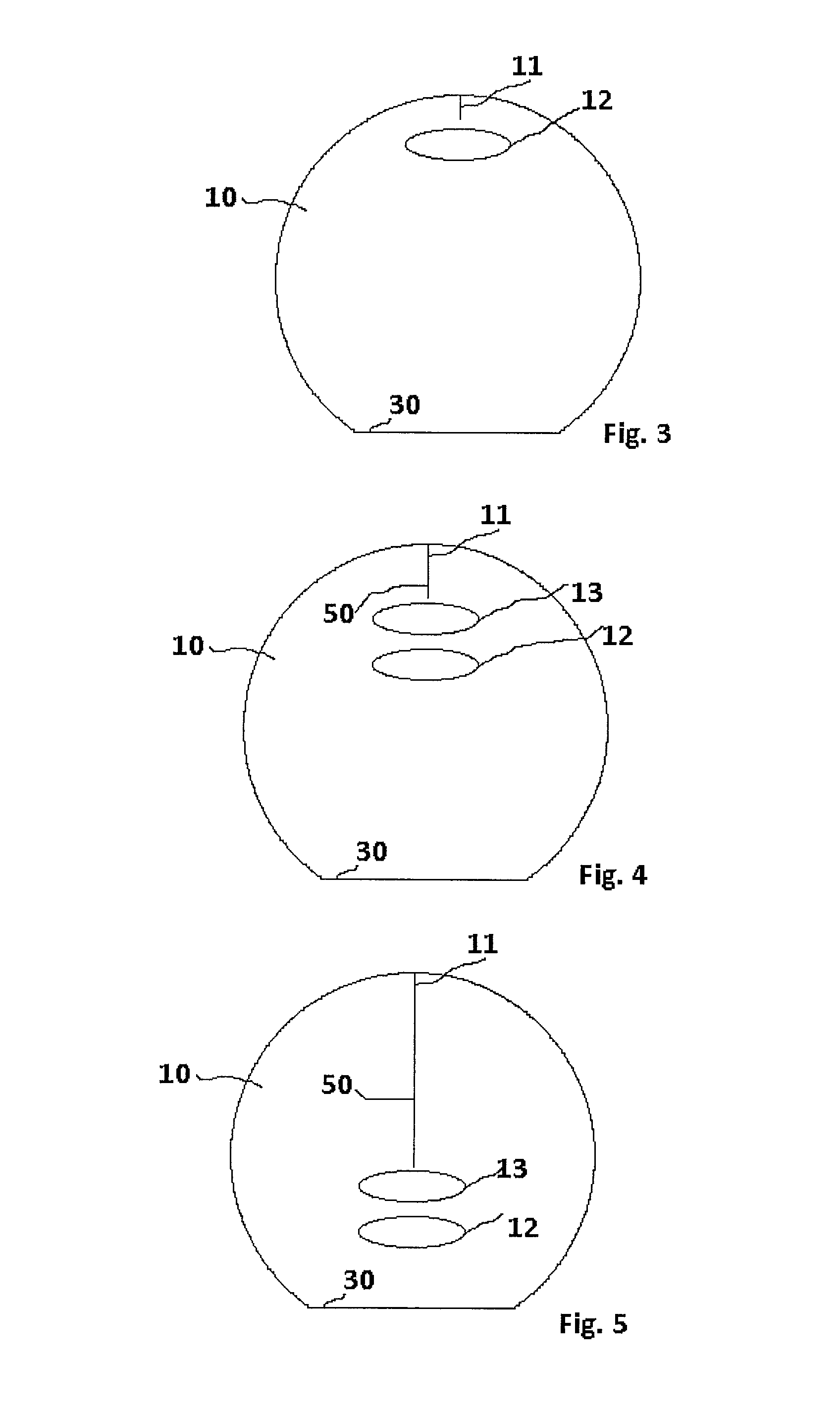
[0011]FIG. 1 shows a conventional process step in the manufacture of diodes from a semiconductor material. Normally, diodes are manufactured in that a semiconductor crystal wafer 10, for example a silicon wafer, is used, and then a p-n or an n-p junction is produced by a process of diffusion or epitaxy. For example, starting from an n-doped silicon wafer, a p-n junction may be produced by a surface introduction or epitactic growth of a p-type doping. FIG. 1 shows in exemplary fashion a silicon wafer having an n-type doping into which a surface p-doping layer was introduced. The lateral view of FIG. 1 shows an n-doped layer 5 and a surface p-doping layer 4, which form a p-n junction. For the purpose of the description, the side on which p-doping layer 4 is applied is designated as top side 2 and the side of n-doping 5 is designated as bottom side 3. By using large-area semiconductor crystal wafers or silicon wafers, a plurality of diodes may be produced, semiconductor crystal wafer 1...


PUM


Abstract

In a method for manufacturing a diode, a semiconductor crystal wafer is used to produce a p-n or n-p junction, which extends in planar fashion across the top side of a semiconductor crystal wafer. Separation edges form perpendicularly to the top side of the semiconductor crystal wafer, which edges extend across the p-n or n-p junction. The separation of the semiconductor crystal wafer is achieved in that, starting from a disturbance, a fissure is propagated by local heating and local cooling of the semiconductor crystal wafer. The separation fissure thus formed extends along crystal planes of the semiconductor crystal, which avoids the formation of defects in the area of the p-n or n-p junction.

Description

BACKGROUND OF THE INVENTION[0001]1. Field of the Invention[0002]The present application relates to a method for manufacturing a diode and to a diode that has a p-n or n-p junction.[0003]2. Description of the Related Art[0004]Normally, such diodes are manufactured in that a semiconductor crystal wafer, for example a silicon wafer, is used in order to produce a p-n or n-p junction by the processes of diffusion or epitaxy. This junction is normally developed in a planar manner on a top side of the semiconductor crystal wafer, and, in a subsequent step, the semiconductor crystal wafer is separated into a plurality of individual diode chips. In the process, separation cuts are introduced, which extend from the top side of the semiconductor crystal wafer to the bottom side, and thus the semiconductor crystal wafer is separated into a great number of individual diode chips. Normally, the separation of the semiconductor crystal wafers occurs by a sawing process. Such a sawing process produc...

Claims


Application Information

Patent Timeline
Patent Type & Authority Patents(United States)
IPC IPC(8): H01L21/78H01L21/44H01L21/301H01L21/50H01L21/00H01L29/861H01L21/48H01L29/66H01L21/30H01L21/76H01L21/46H01L29/32
CPCH01L29/861H01L29/6609H01L29/32H01L29/66136
Inventor SPITZ, RICHARDGOERLACH, ALFREDKOLB, ROBERT
Owner ROBERT BOSCH GMBH
Features
  • R&D
  • Intellectual Property
  • Life Sciences
  • Materials
  • Tech Scout
  • Unparalleled Data Quality
  • Higher Quality Content
  • 60% Fewer Hallucinations
Learn More