Check patentability & draft patents in minutes with Patsnap Eureka AI!

Process for manufacturing buried hetero-structure laser diodes

a laser diode and heterostructure technology, applied in lasers, semiconductor lasers, nanotechnology, etc., can solve the problems of low heat dissipation, difficult to extend an upper electrode to difficult to extend an upper electrode to a region an a side surface of the semiconductor mesa, so as to achieve the effect of further enhancing the breakdown voltage properties of buried heterostructure laser diodes

Inactive Publication Date: 2015-02-17
SUMITOMO ELECTRIC IND LTD
View PDF22 Cites 0 Cited by
  • Summary
  • Abstract
  • Description
  • Claims
  • Application Information

AI Technical Summary

Benefits of technology

This configuration enhances heat dissipation properties of BH LDs while maintaining high breakdown voltage, effectively addressing the limitations of conventional manufacturing processes by allowing heat generated during laser oscillation to be dissipated efficiently towards the side surface of the semiconductor mesa.

Problems solved by technology

Buried hetero-structure laser diodes (BH LDs) obtained by such conventional production processes have a problem in that the heat dissipation properties of the buried hetero-structure laser diodes are low.
Accordingly, it is difficult to extend an upper electrode to a region an a side surface of the semiconductor mesa.
Low heat dissipation properties are ascribed to such a structural problem.
In particular, a quantum cascade laser (QCL) requires a relatively large injection current of about 0.5 A to 1 A, thus resulting in a large amount of heat generated in the active layer.

Method used


Image

  • Process for manufacturing buried hetero-structure laser diodes
  • Process for manufacturing buried hetero-structure laser diodes
  • Process for manufacturing buried hetero-structure laser diodes

Examples


first embodiment

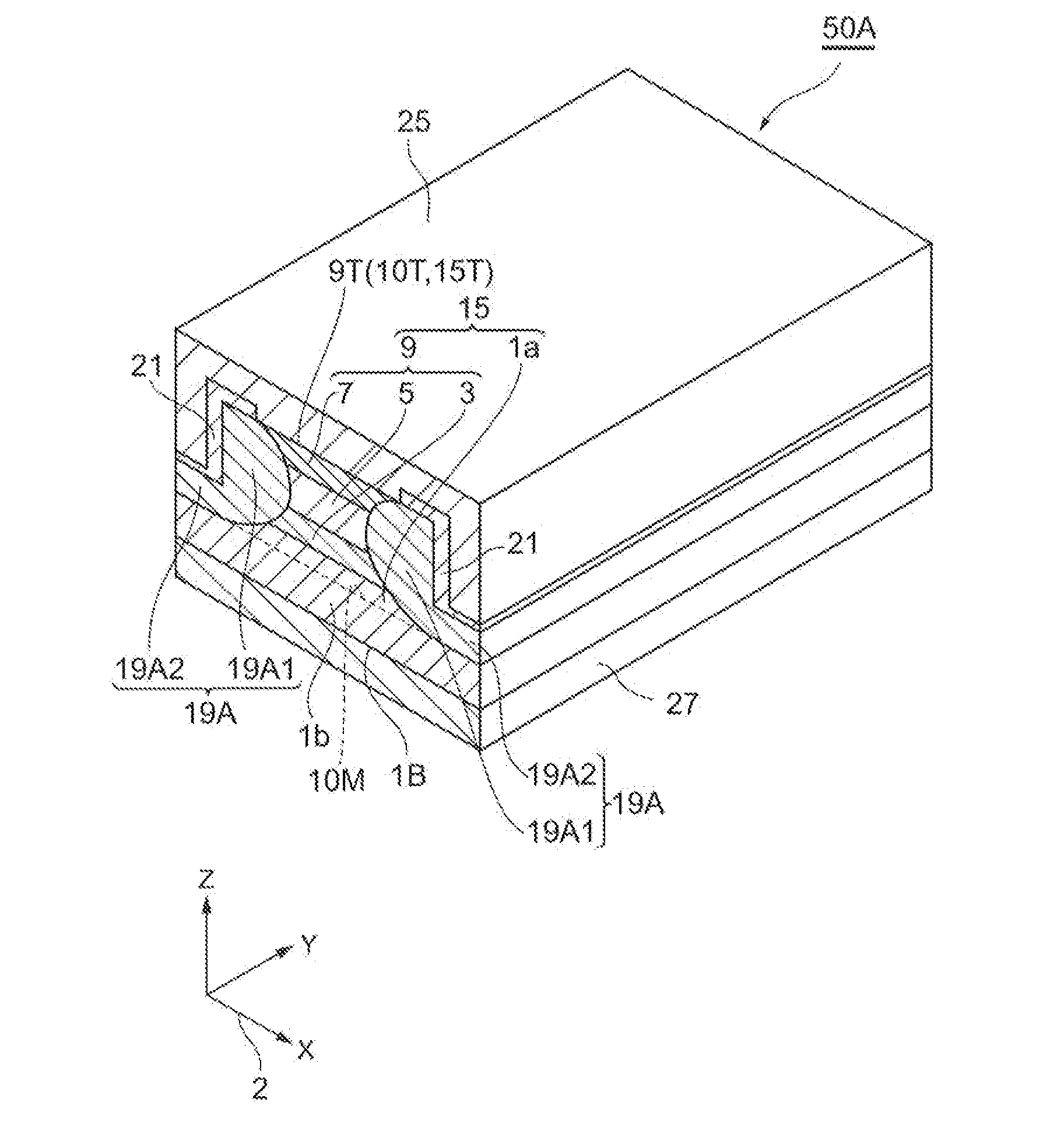
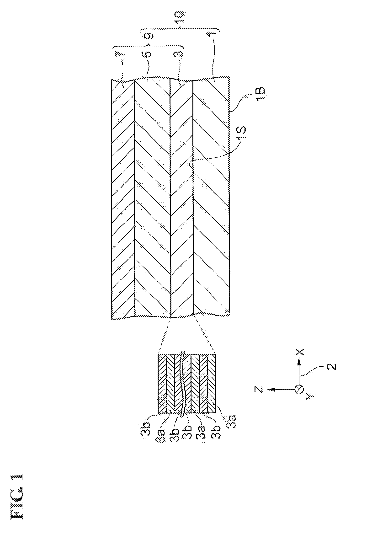
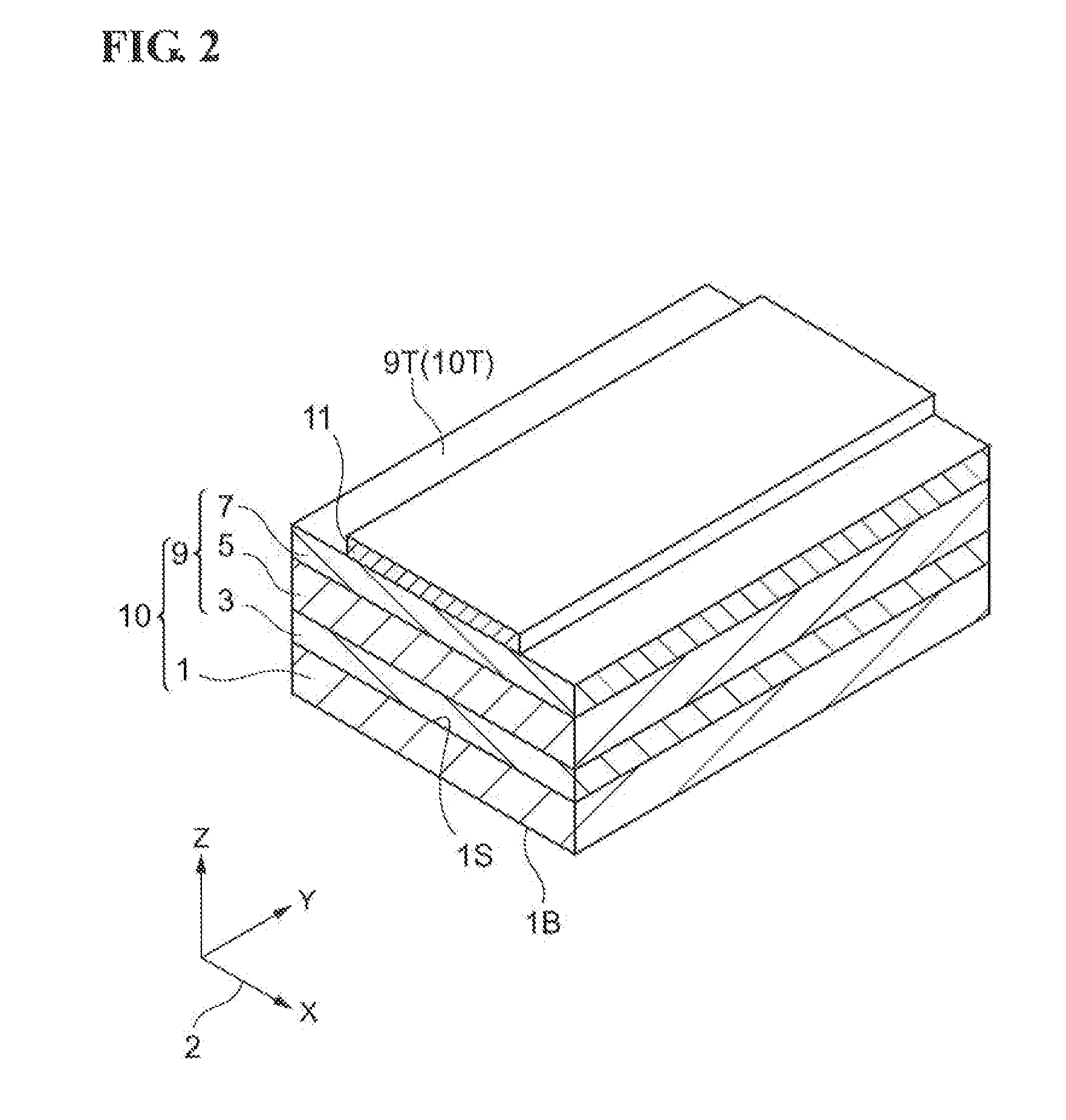
[0044]FIGS. 1 and 3 to 7 are cross sectional views for explaining a process for manufacturing buried hetero-structure laser diodes according to a first embodiment. FIG. 2 is a cross sectional perspective view for explaining a process for manufacturing buried hetero-structure laser diodes according to the first embodiment. FIG. 8 is a perspective view for explaining a process for manufacturing buried hetero-structure laser diodes according to the first embodiment.

[0045]The process for manufacturing buried hetero-structure laser diodes according to this embodiment mainly includes a stacked semiconductor layer forming step, a mask layer forming step, a semiconductor structure etching step, a buried layer forming step, a passivation film forming step and an electrode forming step.

(Stacked Semiconductor Layer Forming Step)

[0046]First, a stacked semiconductor layer forming step is carried out. In this step; as illustrated in FIG. 1, a stacked semiconductor layer 9 including an, active lay...

second embodiment

[0082]Next, a second embodiment of the processes for manufacturing buried hetero-structure laser diodes and the buried hetero-structure laser diodes will be described. The second and later embodiments will be mainly described focusing on the differences from the first embodiment.

[0083]FIGS. 9 to 11 are cross sectional views for explaining a process for manufacturing buried hetero-structure laser diodes according to the second embodiment. FIG. 12 is a perspective view for explaining a process for manufacturing buried hetero-structure laser diodes according to the second embodiment.

[0084]The main difference between the second embodiment and the first embodiment is the contents of the buried layer forming step. In this embodiment, a stacked semiconductor layer forming step to a semiconductor structure etching step are the same as the stacked semiconductor layer forming step to the semiconductor structure etching step in the first embodiment.

[0085]As illustrated in FIG. 9, an etched reg...

third embodiment

[0098]Next, a third embodiment of the processes for manufacturing buried hetero-structure laser diodes and the buried hetero-Structure laser diodes will be described.

[0099]FIGS. 13 to 15 are cross sectional views for explaining a process for manufacturing buried hetero-structure laser diodes according to the third embodiment. FIG. 16 is a perspective view for explaining a process for manufacturing bulled hetero-structure laser diodes according to the third embodiment.

[0100]The main difference between the third embodiment and the first embodiment is the contents of the buried layer forming step. In this embodiment, a principal surface 1S of a semiconductor substrate 1 is a (100) plane. Further, the first direction is a [011] direction of the semiconductor substrate 1. Thus, in the mask layer forming step, a mask layer 11 is formed on a stacked semiconductor layer 9 so as to extend along the [011] direction of the semiconductor substrate 1.

[0101]As illustrated in FIG. 13, an etched re...


PUM


Abstract

A process for manufacturing buried hetero-structure laser diodes includes the steps of forming a stacked semiconductor layer on a substrate; forming a mask layer on the stacked semiconductor layer; forming a semiconductor mesa by etching the stacked semiconductor layer through the mask layer; forming an overhang of the mask layer by selectively etching the stacked semiconductor layer of the semiconductor mesa; selectively growing a buried layer on a side surface of the semiconductor mesa while leaving the mask layer on the semiconductor mesa; forming a lateral portion of the buried layer, the lateral portion having a side surface adjacent to the side surface of the semiconductor mesa; after forming the lateral portion of the buried layer, removing the mask layer on the semiconductor mesa; and forming an electrode on a top surface of the semiconductor mesa and on the side surface of the lateral portion of the buried layer.

Description

BACKGROUND OF THE INVENTION[0001]1. Field of the Invention[0002]The present invention relates to a process for manufacturing buried hetero-structure (BH) laser diodes (LD).[0003]2. Description, of the Related Art[0004]Patent Literature 1 (US Application Publication No. 2008 / 0219312) discloses a quantum cascade laser (QCL) device having a buried hetero-structure. The quantum cascade laser device described in the patent literature 1 has a stripe-shaped mesa structure extending along a predetermined direction of a principal surface of a substrate. Further; the cross-section of the mesa structure in a direction perpendicular to the predetermined direction has a rectangle shape or an inverted mesa shape. With such a configuration, the quantum cascade laser device has high slope efficiency and operates with a stable single transverse mode.[0005]In general, a process for the manufacturing of a buried hetero-structure laser diode (BH LD) includes a step of growing a stacked semiconductor la...

Claims


Application Information

Patent Timeline
Patent Type & Authority Patents(United States)
IPC IPC(8): H01L21/00H01S5/024H01S5/042H01S5/20H01S5/22H01S5/227H01S5/34
CPCH01S5/2086H01S5/2275H01S5/02476H01S5/0425H01S5/2201H01S5/3401H01S5/2224H01S2301/176H01S2304/04B82Y20/00H01S5/04252H01S5/04254
Inventor TSUJI, YUKIHIRO
Owner SUMITOMO ELECTRIC IND LTD
Features
  • R&D
  • Intellectual Property
  • Life Sciences
  • Materials
  • Tech Scout
  • Unparalleled Data Quality
  • Higher Quality Content
  • 60% Fewer Hallucinations
Learn More