Check patentability & draft patents in minutes with Patsnap Eureka AI!

On-chip electronic device and method for manufacturing the same

a technology of electronic devices and on-chip inductors, which is applied in the direction of semiconductor devices, semiconductor/solid-state device details, and inductance, etc., can solve the problems of increasing the occupied area, unfavorable miniaturization of on-chip inductors, and how to effectively increase the inductance, etc., to achieve simple structure, increase in the effect of inductance efficiency, and reduce the occupied area

Inactive Publication Date: 2015-02-17
NAT CHIAO TUNG UNIV
View PDF3 Cites 0 Cited by
  • Summary
  • Abstract
  • Description
  • Claims
  • Application Information

AI Technical Summary

Benefits of technology

[0006]An objective of the present invention is to provide an on-chip electronic device and a method for manufacturing the same, which uses a plurality of magnetic bodies disposed in a plurality of voids in a porous layer as the core of the magnetic inductance for increasing inductance efficiency and reducing occupied area.
[0007]Another objective of the present invention is to provide an on-chip electronic device and a method for manufacturing the same, which has a simple structure with a manufacturing method compatible with the CMOS process, and hence reducing the cost.
[0008]Still another objective of the present invention is to provide an on-chip electronic device and a method for manufacturing the same, which has a high-intensity anisotropy magnetic field, and hence the magnetic resonance (MR) frequency is increased.
[0009]The on-chip electronic device according to the present invention comprises a substrate, a porous layer, a plurality of magnetic bodies, and an electronic member layer. The manufacturing method according to the present invention comprises providing the substrate, forming the porous layer with a plurality of voids on the substrate, forming the plurality of magnetic bodies in the plurality of voids, and forming the electronic member layer on the porous layer. Because the plurality of magnetic bodies is used as the core of the magnetic inductance, the inductance efficiency of the on-chip electronic device is increased effectively while the occupied area is reduced effectively. Besides, because the manufacturing method according to the present invention is compatible with the current CMOS process, the manufacturing cost can be lowered.
[0010]The manufacturing method according to the present invention further comprises providing the substrate, forming a electronic member layer on the substrate, forming a porous layer with a plurality of voids on the electronic member layer, and forming a plurality of magnetic bodies in the plurality of voids. Because the plurality of magnetic bodies is used as the core of the inductance efficiency, the inductance efficiency of the on-chip electronic device is increased effectively while the occupied area is reduced effectively.

Problems solved by technology

All of the current electronic products pursue miniaturization and are fastidious about lightness and thinness.
The method for increasing the inductance of an on-chip inductor is mostly to increase the number of turns of the inductor, which will increase the occupied area, and hence is unfavorable for miniaturization of the on-chip inductor.
Thereby, how to increase effectively the inductance is still a major issue for developing the on-chip inductor.

Method used


Image

  • On-chip electronic device and method for manufacturing the same
  • On-chip electronic device and method for manufacturing the same
  • On-chip electronic device and method for manufacturing the same

Examples


Embodiment Construction

[0023]In order to make the structure and characteristics as well as the effectiveness of the present invention to be further understood and recognized, the detailed description of the present invention is provided as follows along with embodiments and accompanying figures.

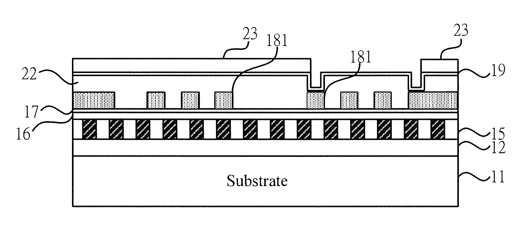
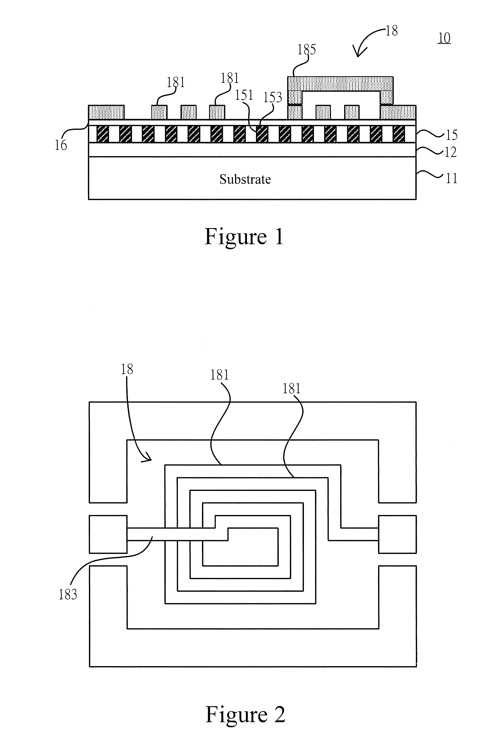
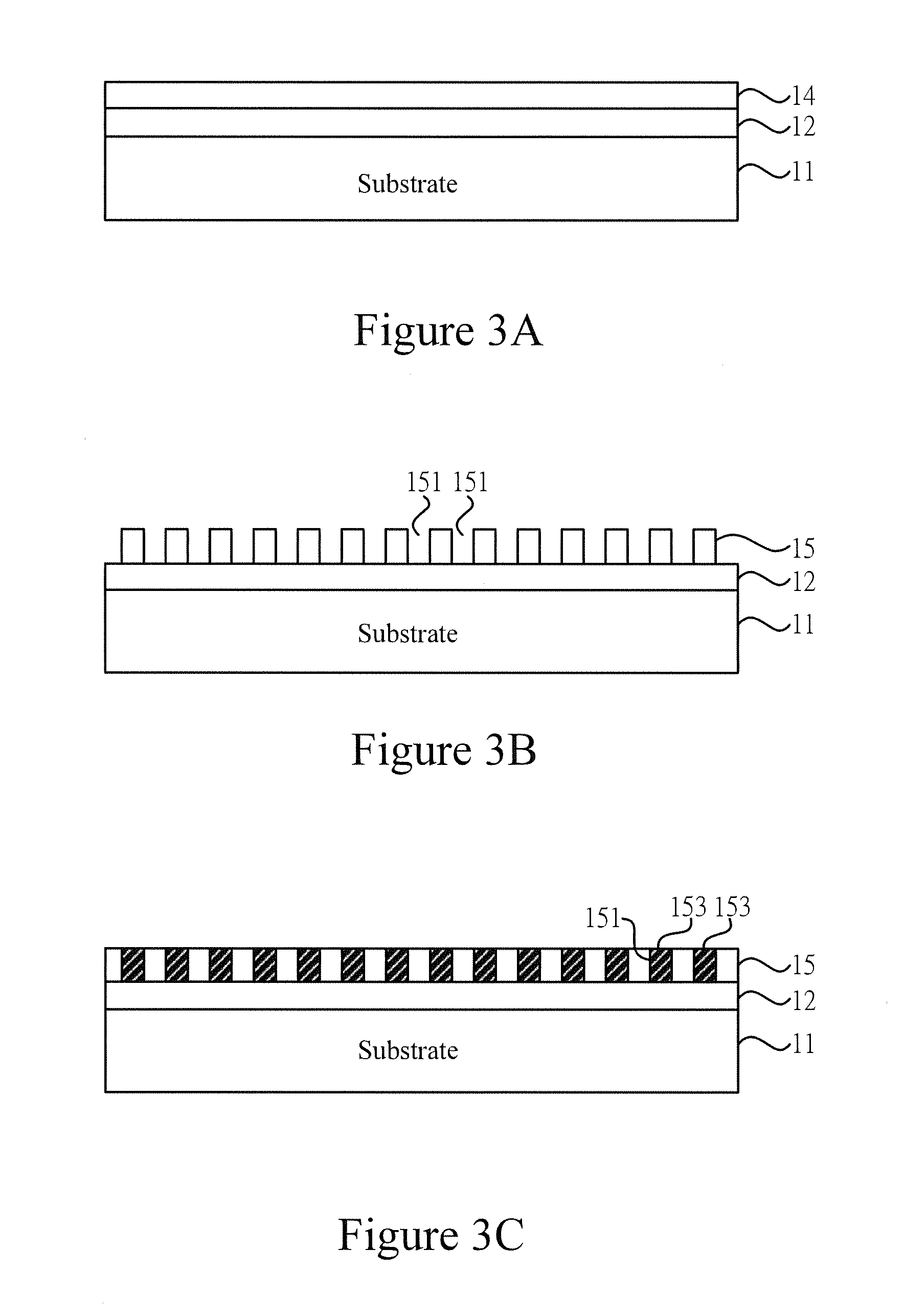
[0024]FIG. 1 shows a structure of the on-chip electronic device according to a preferred embodiment of the present invention. As shown in the figure, the on-chip electronic device 10 according to the present invention is an inductor, which comprises a substrate 11, a porous layer 15, a plurality of magnetic bodies 153, and electronic member layer 18. The porous layer 15 is disposed on the substrate 11 and has a plurality of voids 151 thereon. The plurality of magnetic bodies 153 is disposed in the plurality of voids 151. A preferred embodiment of the porous layer 15 of the on-chip electronic device according to the present invention is a nanometer porous layer. The material of the magnetic bodies 153 can be any con...


PUM


Abstract

The present invention relates to an on-chip electronic device and a method for manufacturing the same. The on-chip electronic device according to the present invention comprises a substrate, a porous layer, a plurality of magnetic bodies, and an electronic member layer. The porous layer is disposed on the substrate and has a plurality of voids; each of the plurality of magnetic bodies is disposed in the plurality of voids, respectively; and the electronic member layer is disposed on one side of the porous layer, such as upper side of or lower sider of the porous layer. Because the plurality of magnetic bodies is used as the core of the inductance, the inductance is increased effectively and the area of the on-chip electronic device is reduced. Besides the manufacturing method according to the present invention is simple and compatible with the current CMOS process, the manufacturing cost can be lowered.

Description

REFERENCE TO RELATED APPLICATION[0001]This Application is being filed as a Continuation-in-Part of patent application Ser. No. 12 / 607,433, filed 28 Oct. 2009, currently pending.FIELD OF THE INVENTION[0002]The present invention relates to a chip structure, and particularly to an on-chip electronic device and a method for manufacturing the same.BACKGROUND OF THE INVENTION[0003]With the progress of modern technologies, the coming of information era, and the prosperous development of network, various electronic products are developed for satisfying people's demand. The functions of the electronic products are becoming powerful and complete increasingly, and thus bringing convenience for people's lives. All of the current electronic products pursue miniaturization and are fastidious about lightness and thinness. Under high-density packaging, the size of the required electronic devices is becoming relatively smaller, particularly for radio-frequency integrated circuits (RFICs) applied in ...

Claims


Application Information

Patent Timeline
Patent Type & Authority Patents(United States)
IPC IPC(8): H01L27/08H01L23/522H01L23/532H01L49/02
CPCH01L28/10H01L23/5227H01L23/5329H01L2924/0002H01L2924/00
Inventor CHENG, YU-TINGCHAO, TZU-YUANCHEN, KUAN-MINGHSU, HSIN-FU
Owner NAT CHIAO TUNG UNIV
Features
  • R&D
  • Intellectual Property
  • Life Sciences
  • Materials
  • Tech Scout
  • Unparalleled Data Quality
  • Higher Quality Content
  • 60% Fewer Hallucinations
Learn More