Check patentability & draft patents in minutes with Patsnap Eureka AI!

Power rail layout for dense standard cell library

a technology of power rails and standard cell libraries, applied in the direction of specific program execution arrangements, instruments, program control, etc., can solve the problem of limited performance of standard semiconductor cell libraries

Inactive Publication Date: 2015-05-05
GLOBALFOUNDRIES INC
View PDF6 Cites 13 Cited by
  • Summary
  • Abstract
  • Description
  • Claims
  • Application Information

AI Technical Summary

Benefits of technology

This approach maximizes active area density, reduces power rail width, and enhances performance by allowing for smaller tip-to-tip spacing and more efficient use of space, thereby improving the performance and reliability of standard cells.

Problems solved by technology

Standard semiconductor cell library performance is limited by the current a transistor of a cell can deliver.

Method used


Image

  • Power rail layout for dense standard cell library
  • Power rail layout for dense standard cell library
  • Power rail layout for dense standard cell library

Examples


Embodiment Construction

[0015]Aspects of the present invention and certain features, advantages, and details thereof, are explained more fully below with reference to the non-limiting embodiments illustrated in the accompanying drawings. Descriptions of well-known materials, fabrication tools, processing techniques, etc., are omitted so as to not unnecessarily obscure the invention in detail. It should be understood, however, that the detailed description and the specific examples, while indicating embodiments of the invention, are given by way of illustration only, and are not by way of limitation. Various substitutions, modifications, additions, and / or arrangements within the spirit and / or scope of the underlying inventive concepts will be apparent to those skilled in the art from this disclosure.

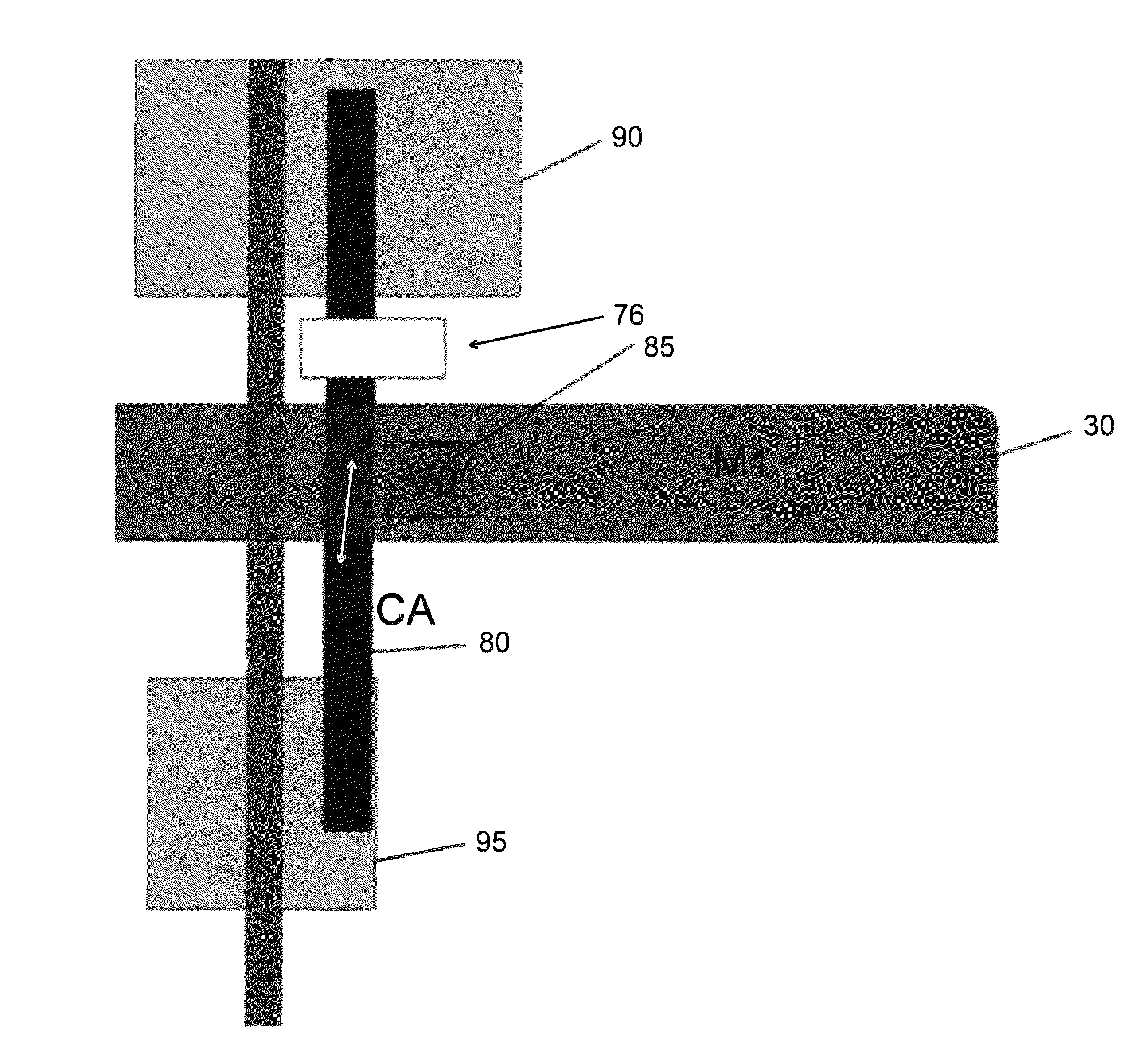
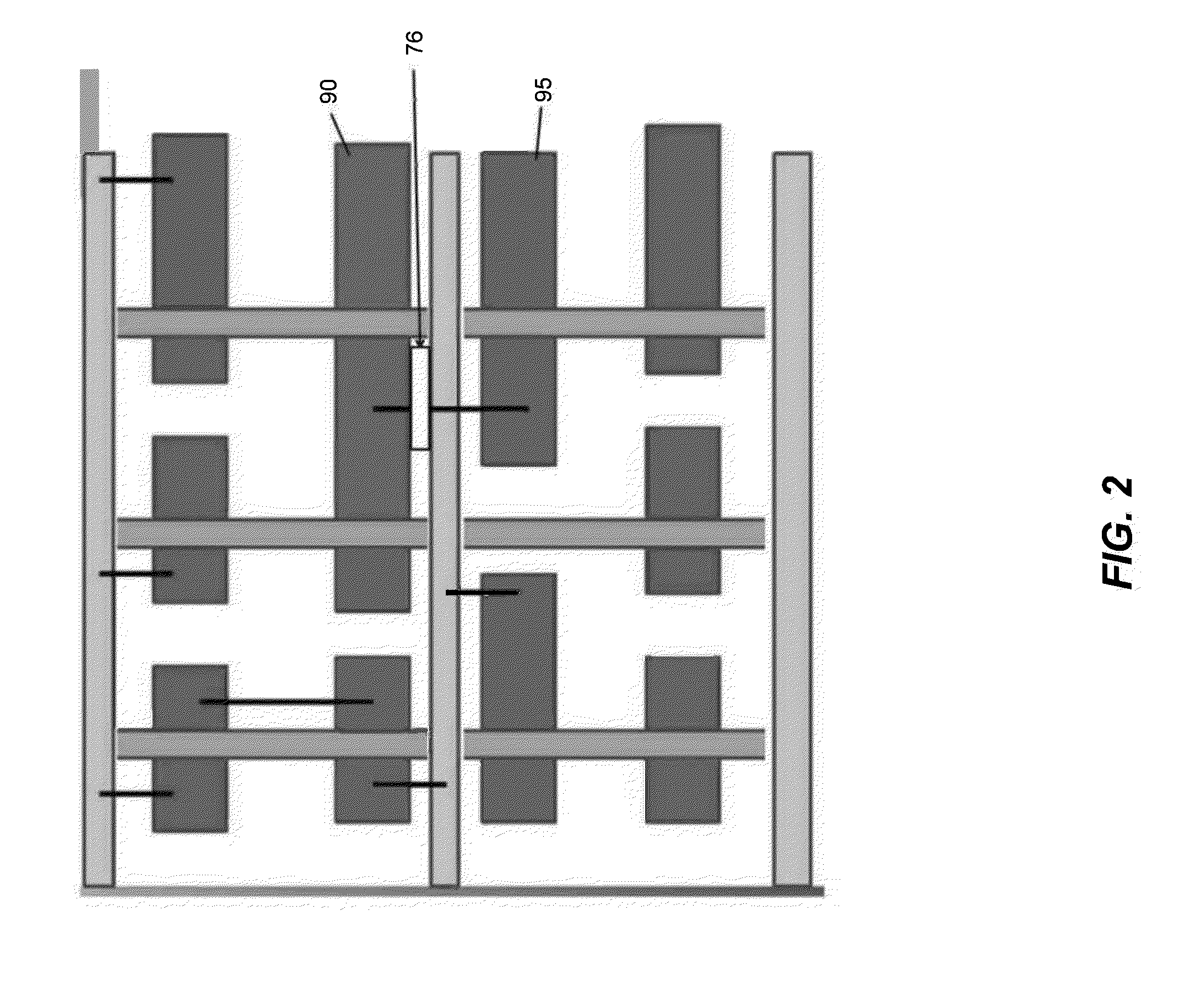
[0016]A schematic diagram of an example of a portion 5 of a FINFET standard cell layout includes active areas 10 (e.g., positive or negative metal oxide semiconductors) is depicted in FIG. 1. Each cell or multip...


PUM


Abstract

A method includes electrically connecting a plurality of cells of a standard cell library to a power rail. A contact area is deposited to connect a first active area and a second active area of a cell of a plurality cells. The first area and the second area are located on opposite sides of the rail and electrically connected to different drains. The contact area is electrically connected to the power rail using a via. The contact area is masked to remove a portion of the contact area to electrically separate the first active are from the second active area.

Description

FIELD OF THE INVENTION[0001]The present invention generally relates to semiconductor devices and methods of fabricating semiconductor devices, and more particularly, to methods of fabricating semiconductor devices using standard semiconductor cell fabrication.BACKGROUND OF THE INVENTION[0002]Standard semiconductor cell fabrication is a method for designing integrated circuits for specific applications. Circuits are designed based on the desired functions using cells from a cell library which are combined and constructed by a placement tool to result in the desired circuits. Standard semiconductor cell library performance is limited by the current a transistor of a cell can deliver. This is proportional to the width of the transistor so it is desirable to enable the transistor to be as wide as possible in a standard cell to deliver high performance circuits.[0003]A typical standard cell loses some active area in two regions including the power rail and the center of the cell where si...

Claims


Application Information

Patent Timeline
Patent Type & Authority Patents(United States)
IPC IPC(8): G06F9/455G06F17/50
CPCG06F17/5077G06F2217/06G06F30/394G06F2111/04G06F2119/06
Inventor TARABBIA, MARCCHEN, NORMANLIU, JIANHINDAWY, NADER MAGDYNEOGI, TUHIN GUHARASHED, MAHBUBMITTAL, ANURAG
Owner GLOBALFOUNDRIES INC
Features
  • R&D
  • Intellectual Property
  • Life Sciences
  • Materials
  • Tech Scout
  • Unparalleled Data Quality
  • Higher Quality Content
  • 60% Fewer Hallucinations
Learn More