Supercharge Your Innovation With Domain-Expert AI Agents!

Sputter and surface modification etch processing for metal patterning in integrated circuits

a technology of integrated circuits and surface modification, which is applied in the direction of semiconductor devices, semiconductor/solid-state device details, electrical apparatus, etc., can solve the problems of reentrant reactive ion etching profiles, poor liner/seed coverage on the walls of trenches, and damascene processing that is not always compatible with the trend toward smaller feature sizes

Inactive Publication Date: 2015-06-23
GLOBALFOUNDRIES INC
View PDF41 Cites 2 Cited by
  • Summary
  • Abstract
  • Description
  • Claims
  • Application Information

AI Technical Summary

Benefits of technology

The process enables the fabrication of CMOS devices with feature sizes less than 40 nanometers and pitches less than 100 nanometers, resulting in minimal voids and defects, maximized grain growth, and reduced resistivity, maintaining conductivity and minimizing surface roughening.

Problems solved by technology

Conventional damascene processing such as that described above is not always compatible with the trend toward smaller feature sizes in modern complementary metal-oxide-semiconductor (CMOS) technology.
Attempting conventional damascene processing within these parameters often results in poor liner / seed coverage on the walls of the trenches (e.g., as illustrated at 102 in FIG. 1), pinch off at the mouths of the trenches (e.g., as illustrated at 104), and reentrant reactive ion etching profiles (e.g., as illustrated at 106).
Consequently, the copper filling the trenches is subject to voids, defects, and poor adhesion to the trench liners.
Moreover, as the lines narrow in size, the resistivity of the copper is increased (due to, for example, the thickness of the liner relative to the thickness of the copper, the small copper grain size, and copper grain boundary and surface scattering phenomena), resulting in decreased IC performance.

Method used


Image

  • Sputter and surface modification etch processing for metal patterning in integrated circuits
  • Sputter and surface modification etch processing for metal patterning in integrated circuits
  • Sputter and surface modification etch processing for metal patterning in integrated circuits

Examples


Embodiment Construction

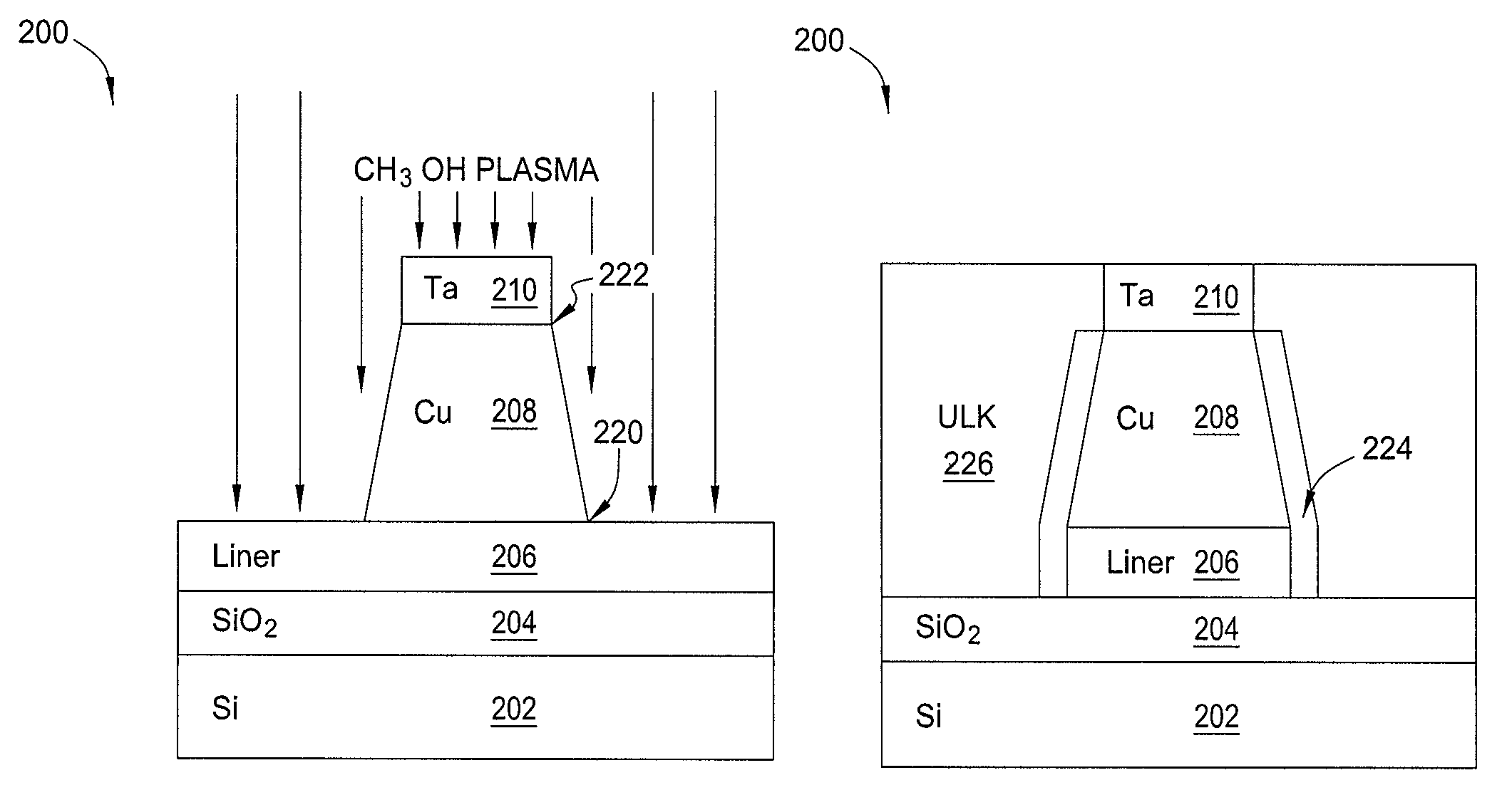
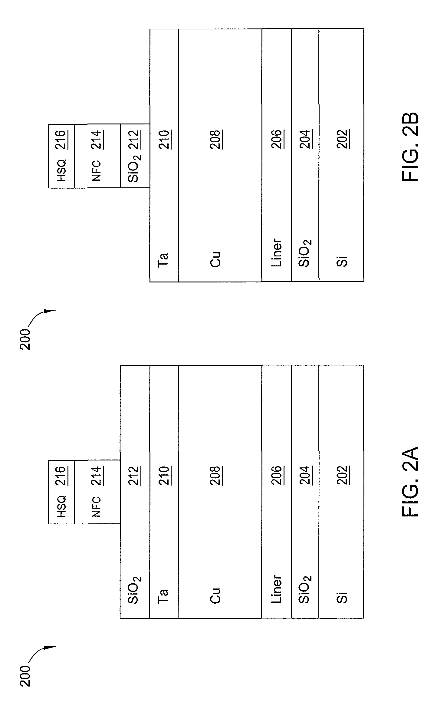
[0011]In one embodiment, the invention is a method and apparatus for metal patterning using a sputter etch process. Embodiments of the invention pattern fine metal lines on an insulating layer of an integrated circuit via a subtractive process (i.e., a process that creates a desired structure by removing material rather than by adding material). In a particular embodiment, the subtractive process uses methanol etch chemistry. The methanol etch process may comprise a single-step process including only a methanol plasma etch, or a two-step process including methanol plasma etch followed by a second plasma etch using a different plasma chemistry. The disclosed process maximizes metal grain growth and minimizes metal resistivity. In addition, the disclosed process allows for flexibility in the choice of materials used for trench liners and minimizes low-k / ultra-low-k damage phenomena due to hard mask stripping and chemical mechanical polishing.

[0012]FIGS. 2A-2I are schematic diagrams il...


PUM


Abstract

One embodiment of an integrated circuit includes a plurality of semiconductor devices and a plurality of conductive lines connecting the plurality of semiconductor devices, wherein at least some of the plurality of conductive lines have pitches of less than one hundred nanometers and sidewall tapers of between approximately eighty and ninety degrees. Another embodiment of an integrated circuit includes a plurality of semiconductor devices and a plurality of conductive lines connecting the plurality of semiconductor devices, wherein at least some of the plurality of conductive lines are fabricated by providing a layer of conductive metal in a multi-layer structure fabricated upon a wafer and sputter etching the layer of conductive metal using a methanol plasma, wherein a portion of the layer of conductive metal that remains after the sputter etching forms the one or more conductive lines.

Description

CROSS REFERENCE TO RELATED APPLICATIONS[0001]This application is a continuation of U.S. patent application Ser. No. 13 / 671,186, filed Nov. 7, 2012, which is herein incorporated by reference in its entirety.BACKGROUND OF THE INVENTION[0002]The present invention relates generally to integrated circuits and relates more specifically to metal patterning processes for use in manufacturing integrated circuits.[0003]Integrated circuits (ICs) commonly use copper interconnects (or “lines”) to connect transistors and other semiconductor devices on the ICs. These interconnects are typically fabricated using an additive damascene process in which an underlying insulating layer (e.g., silicon oxide) is patterned with open trenches. FIG. 1, for example, is a schematic diagram illustrating a trench 100 that may be formed in the insulating layer during IC fabrication. A subsequent deposition of copper on the insulating layer fills the trenches with copper. The copper is removed to the top of the in...

Claims


Application Information

Patent Timeline
Patent Type & Authority Patents(United States)
IPC IPC(8): H01L27/092H01L21/768H01L21/3213
CPCH01L27/092H01L21/32131H01L21/32136H01L21/32139H01L21/76885H01L21/76852H01L2924/0002H01L2924/00H01L21/02109H01L21/31111H01L21/76856H01L21/823871H01L23/535
Inventor CABRAL, JR., CYRILFLETCHER, BENJAMIN L.FULLER, NICHOLAS C. M.JOSEPH, ERIC A.MIYAZOE, HIROYUKI
Owner GLOBALFOUNDRIES INC
Features
  • R&D
  • Intellectual Property
  • Life Sciences
  • Materials
  • Tech Scout
  • Unparalleled Data Quality
  • Higher Quality Content
  • 60% Fewer Hallucinations
Learn More