Check patentability & draft patents in minutes with Patsnap Eureka AI!

Wiring board for electronic parts inspecting device and its manufacturing method

a technology for electronic parts and inspection devices, applied in solid-state devices, measurement instrument housings, instruments, etc., can solve the problem that multi-layer ceramic boards cannot be manufactured and delivered in a short amount of tim

Active Publication Date: 2015-10-27
NGK SPARK PLUG CO LTD
View PDF60 Cites 0 Cited by
  • Summary
  • Abstract
  • Description
  • Claims
  • Application Information

AI Technical Summary

Benefits of technology

This approach significantly shortens the design and manufacturing time for inspecting circuits, enabling precise and rapid inspection of electronic parts while minimizing production costs and the number of jigs needed.

Problems solved by technology

However, when the inner wirings are provided to the board as in the above probe card, since the inner wirings need to be designed which respectively correspond to electronic parts to be inspected between layers of a multi-layer ceramic board, it is time consuming to design such a multi-layer ceramic board and a jig is required for forming via conductors or the inner wirings at prescribed positions for each ceramic layer.
Accordingly, a problem arises that multi-layer ceramic boards cannot be manufactured and delivered in a short amount of time.

Method used


Image

  • Wiring board for electronic parts inspecting device and its manufacturing method
  • Wiring board for electronic parts inspecting device and its manufacturing method
  • Wiring board for electronic parts inspecting device and its manufacturing method

Examples


Embodiment Construction

[0056]An exemplary embodiment for carrying out the present invention will be described in detail with reference to the drawings.

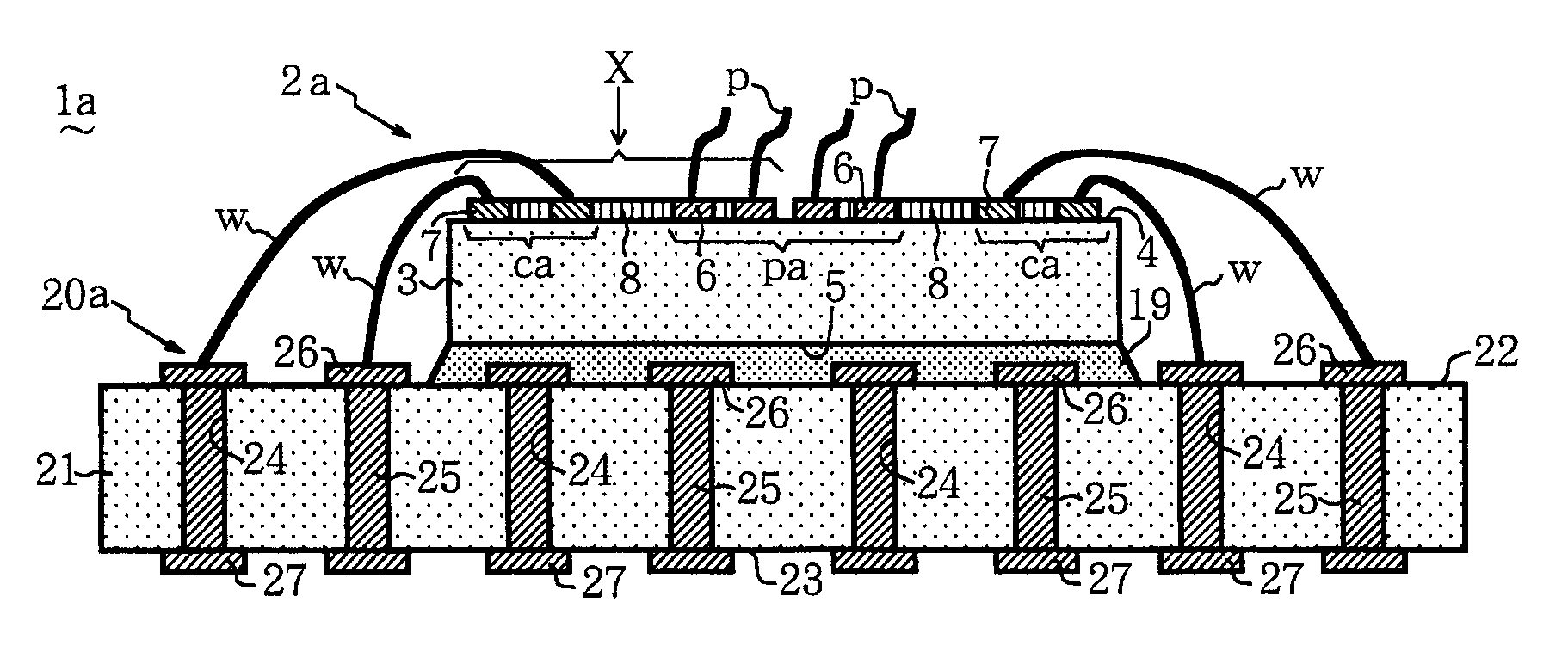
[0057]FIG. 1 is a vertical sectional view showing a wiring board for an electronic parts inspecting device (hereinafter “wiring board”) 1a of one exemplary embodiment according to the present invention. FIG. 2 is an enlarged plane view showing section X of FIG. 1. FIG. 3 is a vertical sectional view taken along a line Y-Y of FIG. 2.

[0058]As shown in FIG. 1, the wiring board 1a includes a flat plate shaped base board 20a and a mounting board 2a mounted on a front surface 22 of the base board 20a.

[0059]The base board 20a includes a board main body 21 made of, for instance, high temperature sintered ceramics (e.g., an insulating material) such as alumina, and having a front surface 22 and a back surface 23 substantially with square forms from a plane view, a plurality of first via conductors 25 formed respectively for a plurality of via holes 24 passing throu...


PUM

PropertyMeasurementUnit
thicknessaaaaaaaaaa
widthaaaaaaaaaa
electric conductivityaaaaaaaaaa

Abstract

A wiring board for an electronic parts inspecting device that can be designed and produced relatively quickly, inexpensively, and with few jigs is provided. In certain embodiments the wiring board includes a base board made of an insulating material having a front surface and a back surface, the base board including a plurality of first via conductors as well as first terminals on the front surface and outer terminals on the back surface that are connected to the ends of the first via conductors, and a mounting board on the front surface of the base board having a front side that includes, a plurality of probe pads, a plurality of second terminals that are electrically connected to the first terminals of the base board, and front surface wirings that connect the probe pads to the second terminals. Lastly, a method of manufacturing the same is provided.

Description

CROSS REFERENCE TO RELATED APPLICATIONS[0001]The present invention claims priority from Japanese Patent Application No. 2011-048522, which was filed on Mar. 7, 2011, and Japanese Patent Application No. 2011-224601, which was filed on Oct. 12, 2011, the disclosures of which are herein incorporated by reference in its entirety.BACKGROUND OF THE INVENTION[0002]1. Field of the Invention[0003]The present invention relates to a wiring board for an electronic parts inspecting device, which is used for inspecting the electric conductivity or other property of an electronic part, and its manufacturing method.[0004]2. Description of Related Art[0005]In order to inspect the electric conductivity or other property of an electronic part, such as an IC chip or an LSI, a probe card is proposed in which a plurality of signal pads are formed for attaching a probe to a part near a central part on a front surface of a board made of an insulating material, such as ceramics. A plurality of inner wirings...

Claims


Application Information

Patent Timeline
Patent Type & Authority Patents(United States)
IPC IPC(8): G01R31/00G01R1/04
CPCG01R1/04G01R1/07378G01R3/00G01R31/2889H01L2224/32225H01L2224/48227H01L2224/73265H01L2224/83385Y10T29/49163H01L2924/00G01R31/28G01R31/50
Inventor ONO, TOMOYOSHIAKITA, KAZUSHIGENOMURA, TOSHIHISA
Owner NGK SPARK PLUG CO LTD
Features
  • R&D
  • Intellectual Property
  • Life Sciences
  • Materials
  • Tech Scout
  • Unparalleled Data Quality
  • Higher Quality Content
  • 60% Fewer Hallucinations
Learn More