A/D conversion circuit and solid-state imaging device
a conversion circuit and solid-state imaging technology, applied in the field of a/d conversion circuit and solid-state imaging device, can solve problems such as errors of 1 lsb or mor
- Summary
- Abstract
- Description
- Claims
- Application Information
AI Technical Summary
Benefits of technology
Problems solved by technology
Method used
Image


Examples
first embodiment
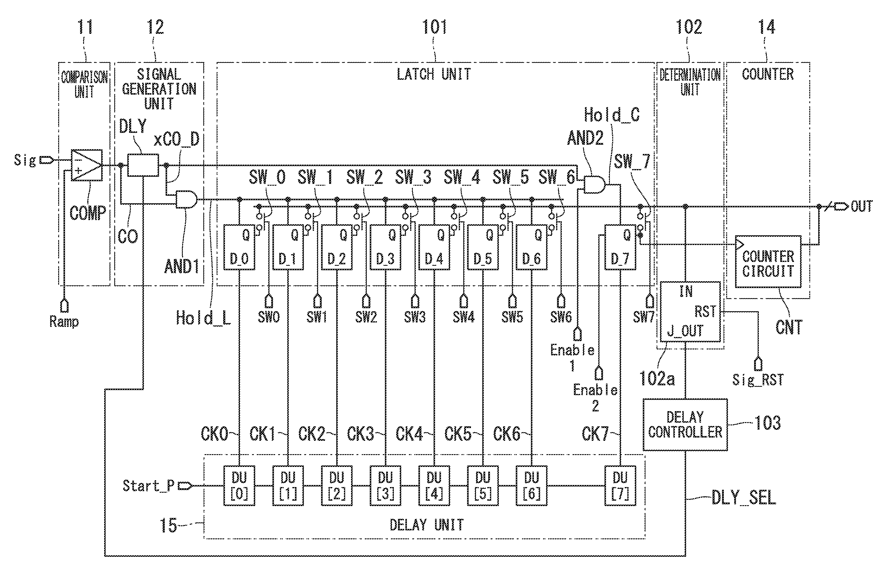
[0053]Firstly, a first embodiment of the present invention will be described. FIG. 1 illustrates an example of the configuration of an A / D conversion circuit according to the present embodiment. Hereinafter, the configuration of the present example will be described. The A / D conversion circuit illustrated in FIG. 1 includes a comparison unit 11, a signal generation unit 12, a latch unit 101, a determination unit 102, a counter 14, a delay unit 15 (a clock generation unit), and a delay controller 103 (a time controller).
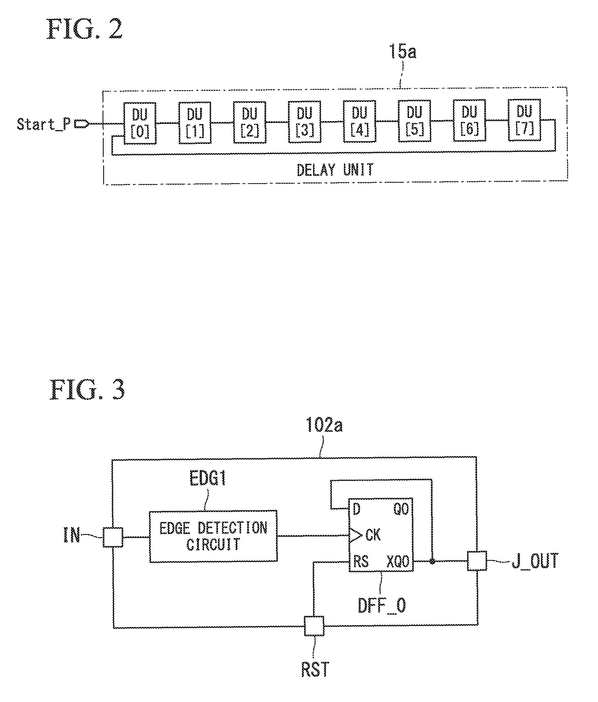
[0054]The delay unit 15 (the clock generation unit) includes a plurality of delay units DU[0] to DU[7] that delay and output an input signal. The delay units DU[0] to DU[7] are serially connected to one another in sequence of the delay unit DU[0], the delay unit DU[1], the delay unit DU[2], . . . , and the delay unit DU[7], and a start pulse Start_P is input to the first delay unit DU[0]. The delay unit DU[0] delays and outputs the input start pulse Start_P, and the d...
second embodiment
[0091]Next, a second embodiment of the present invention will be described. FIG. 6 illustrates an example of the configuration of a solid-state imaging device according to the present embodiment. Hereinafter, the configuration of the present embodiment will be described. A solid-state imaging device 2000 illustrated in FIG. 6 includes an imaging unit 201, a read current source unit 204, an analog unit 205, a column processing unit 206, an operation unit 222, a ramp unit 214, a delay unit 216, a vertical selection unit 218, a controller 220, and a horizontal selection unit 221.
[0092]The imaging unit 201 includes a plurality of unit pixels 202 that are arranged in a matrix form to generate and output a signal corresponding to the amount of incident light. The vertical selection unit 218 selects each row of the imaging unit 201. The read current source unit 204 reads a signal from the imaging unit 201 as a voltage signal. The analog unit 205 includes a sample and hold circuit and the l...
third embodiment
[0165]Next, a third embodiment of the present invention will be described. FIG. 12 illustrates an example of the configuration of a solid-state imaging device according to the present embodiment. In each configuration used in FIG. 12, the same reference numerals are used to designate the same elements as those of FIG. 6, and a description thereof will be omitted here. Hereinafter, each configuration of the present embodiment will be described while focusing on differences from the second embodiment.
[0166]In a solid-state imaging device 300 illustrated in FIG. 12, the ADC unit 207 is divided into three blocks (a first block, a second block, and a third block) every two columns, output signals Jout of the determination units 211 are individually output from the respective blocks, and control signals DLY_SEL are individually output to the respective blocks. In FIG. 12, the output signals Jout from the three blocks are indicated as Jout[2:0] and the control signals DLY_SEL to the three ...
PUM
 Abstract
Description
Claims
Application Information
 - R&D
- Intellectual Property
- Life Sciences
- Materials
- Tech Scout
- Unparalleled Data Quality
- Higher Quality Content
- 60% Fewer Hallucinations
Browse by: Latest US Patents, China's latest patents, Technical Efficacy Thesaurus, Application Domain, Technology Topic, Popular Technical Reports.
© 2025 PatSnap. All rights reserved.Legal|Privacy policy|Modern Slavery Act Transparency Statement|Sitemap|About US| Contact US: help@patsnap.com