Check patentability & draft patents in minutes with Patsnap Eureka AI!

Connector for multi-layered board

a multi-layer board and connector technology, applied in the direction of fixed connections, printed element electric connection formation, coupling device connection, etc., can solve the problems of preventing the miniaturization of multi-layer boards and electronic devices, and the contact stability may not be achieved, so as to prevent the deformation of multi-layer boards, improve contact stability, and minimize the impact

Active Publication Date: 2016-04-19
MOLEX INC
View PDF8 Cites 4 Cited by
  • Summary
  • Abstract
  • Description
  • Claims
  • Application Information

AI Technical Summary

Benefits of technology

This design minimizes the impact of dimensional variations and strength differences in multilayered boards, preventing deformation and enhancing contact stability by distributing reaction forces effectively.

Problems solved by technology

These connectors may impede further miniaturization of multilayered boards and electronic devices.
Therefore, contact stability may not be achieved.

Method used


Image

  • Connector for multi-layered board
  • Connector for multi-layered board
  • Connector for multi-layered board

Examples


first embodiment

[0034]FIG. 2 shows the multilayered board in the connector for a multilayered board according to the Present Disclosure, in which (a) is a top view of the multilayered board, (b) is a front view of the multilayered board, (c) is a bottom view of the multilayered board, and (d) is a side view of the multilayered board. As shown, the multilayered board 2 is a printed circuit board with multiple layers. For example, the multilayered board 2 in the present embodiment is a three-layered printed circuit board. The substrate on the top is the first laminated substrate 2b, the substrate in the middle is the second laminated substrate 2c, and the substrate on the bottom is the third laminated substrate 2d.

[0035]FIG. 3 shows the multilayered board in the connector for a multilayered board according to the first embodiment of the Present Disclosure, in which (a) is an A-A cross-sectional view of the multilayered board, and (b) is an enlarged front view of a column-shaped terminal. As shown, a...

fifth embodiment

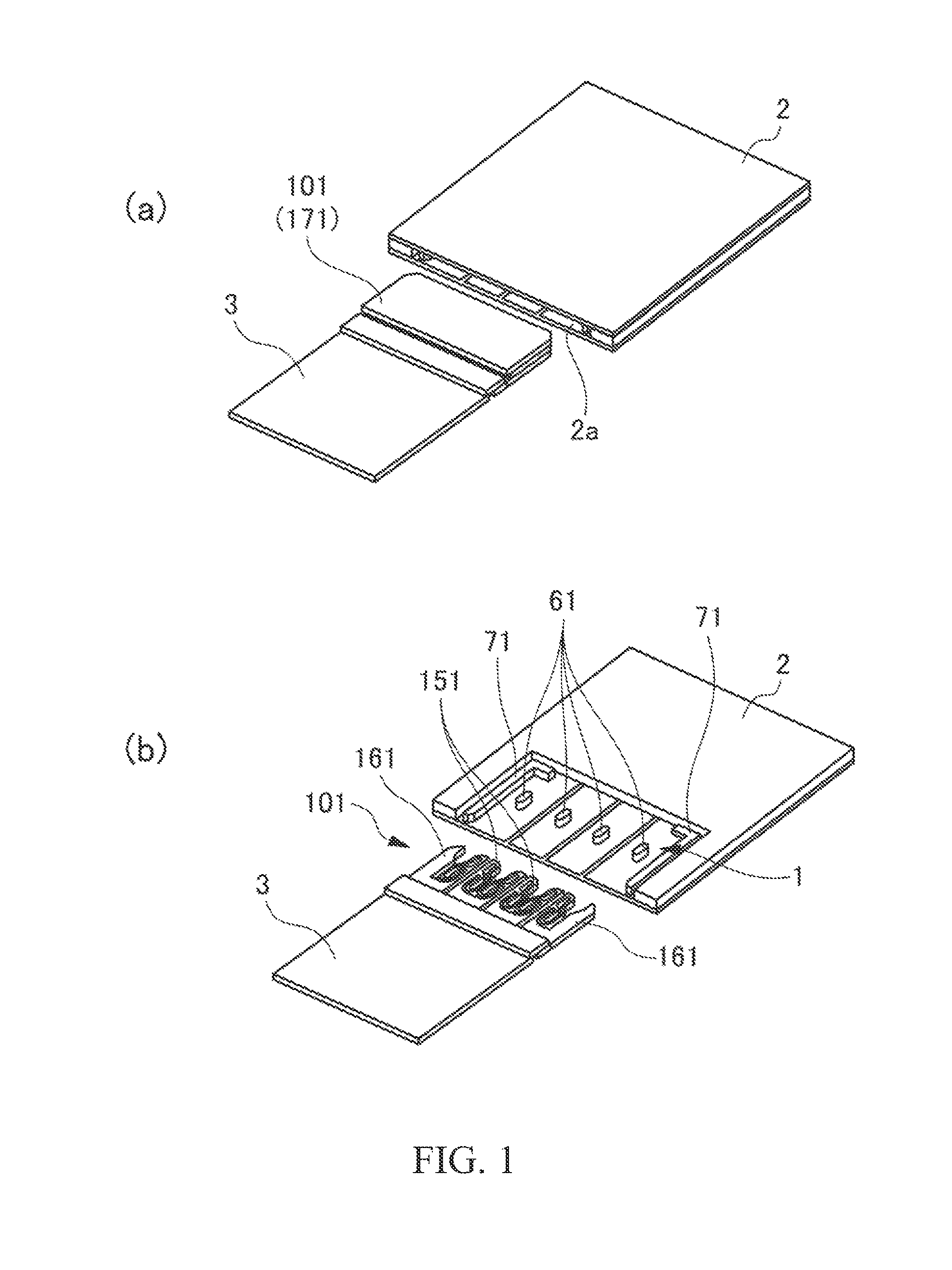
[0067]The connector for a multilayered board includes a retaining structure for retaining two connected flat cables 3 connected to the multilayered board 2 using a single pin 2f. The retaining structure includes an insertion hole 2g formed in the multilayered board 2 so as to vertically pass through the flat cables 3 (cable-side connecting portions 101) inserted from different directions at an overlapping location in plan view, and an engagement hole (not shown) formed in the flat cable 3 (cable-side connecting portion 101) so as to align with the insertion hole 2g when inserted. The pin 2f is inserted into the insertion hole 2g after the cables have been inserted to engage the pin 2f with the engagement holes in the two flat cables 3 and retain both flat cables 3.


PUM


Abstract

A connector for a multilayered board to connect a flat cable to a middle layer of a multilayered board while minimizing the impact due to variations in the dimensional precision and strength of multilayered boards and / or preventing deformation of the multilayered board and improving contact stability. The connector includes a board-side connecting portion and a cable-side connecting portion. The board-side connecting portion includes a column-shaped terminal, and the cable-side connecting portion includes flat terminals. The column-shaped terminal protrudes from the middle layer of the multilayered board in the thickness direction. The flat terminals include resilient contact portions, contacting a side surface portion of the column-shaped terminal from the width direction of the insertion slot in response to insertion of the cable-side connecting portion into the insertion slot.

Description

CROSS REFERENCE TO RELATED APPLICATIONS[0001]The Present Disclosure claims priority to prior-filed Japanese Patent Application No. 2013-065641, entitled “Connector For Multi-Layered Board,” filed on 27 Mar. 2013 with the Japanese Patent Office. The content of the aforementioned Patent Application is fully incorporated in its entirety herein.BACKGROUND OF THE PRESENT DISCLOSURE[0002]The Present Disclosure relates, generally, to a connector for a multilayered board used to connect a flat cable, such as a flexible printed cable, to a middle layer of a multilayered board.[0003]Multilayered boards, which are printed circuit boards formed in layers, are commonly used in electronic devices, such as mobile phones and smartphones, in response to the increasing density of wiring patterns. A flat cable, such as a flexible printed cable, is used to connect a multilayered board to an electronic component module and to connect multilayered boards to each other.[0004]When a flat cable is connected...

Claims


Application Information

Patent Timeline
Patent Type & Authority Patents(United States)
IPC IPC(8): H01R13/62H01R12/52H01R12/79H05K1/11H05K3/36H05K3/32H05K3/40
CPCH01R12/523H01R12/79H05K1/117H05K3/365H05K3/368H05K3/326H05K3/403H05K2201/0367H05K2201/0919H05K2201/09163H05K2201/09863H05K2201/10303H05K2201/10386
Inventor NIITSU, TOSHIHIROHAGA, MOTOHISA
Owner MOLEX INC
Features
  • R&D
  • Intellectual Property
  • Life Sciences
  • Materials
  • Tech Scout
  • Unparalleled Data Quality
  • Higher Quality Content
  • 60% Fewer Hallucinations
Learn More