Sensor having an embedded electrode, and method for manufacturing same
a technology of sensing electrodes and manufacturing methods, which is applied in the direction of measuring devices, instruments, material electrochemical variables, etc., can solve the problems of short-circuit or disconnection of sensing electrodes, defects due to delamination of sensing electrodes, and high manufacturing costs, so as to improve the accuracy of measurement and accuracy. , the effect of easy adjustment of the number
- Summary
- Abstract
- Description
- Claims
- Application Information
AI Technical Summary
Benefits of technology
Problems solved by technology
Method used
Image

Examples
first embodiment
[0047
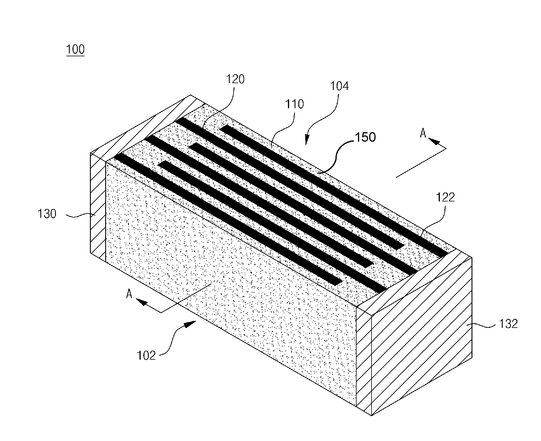
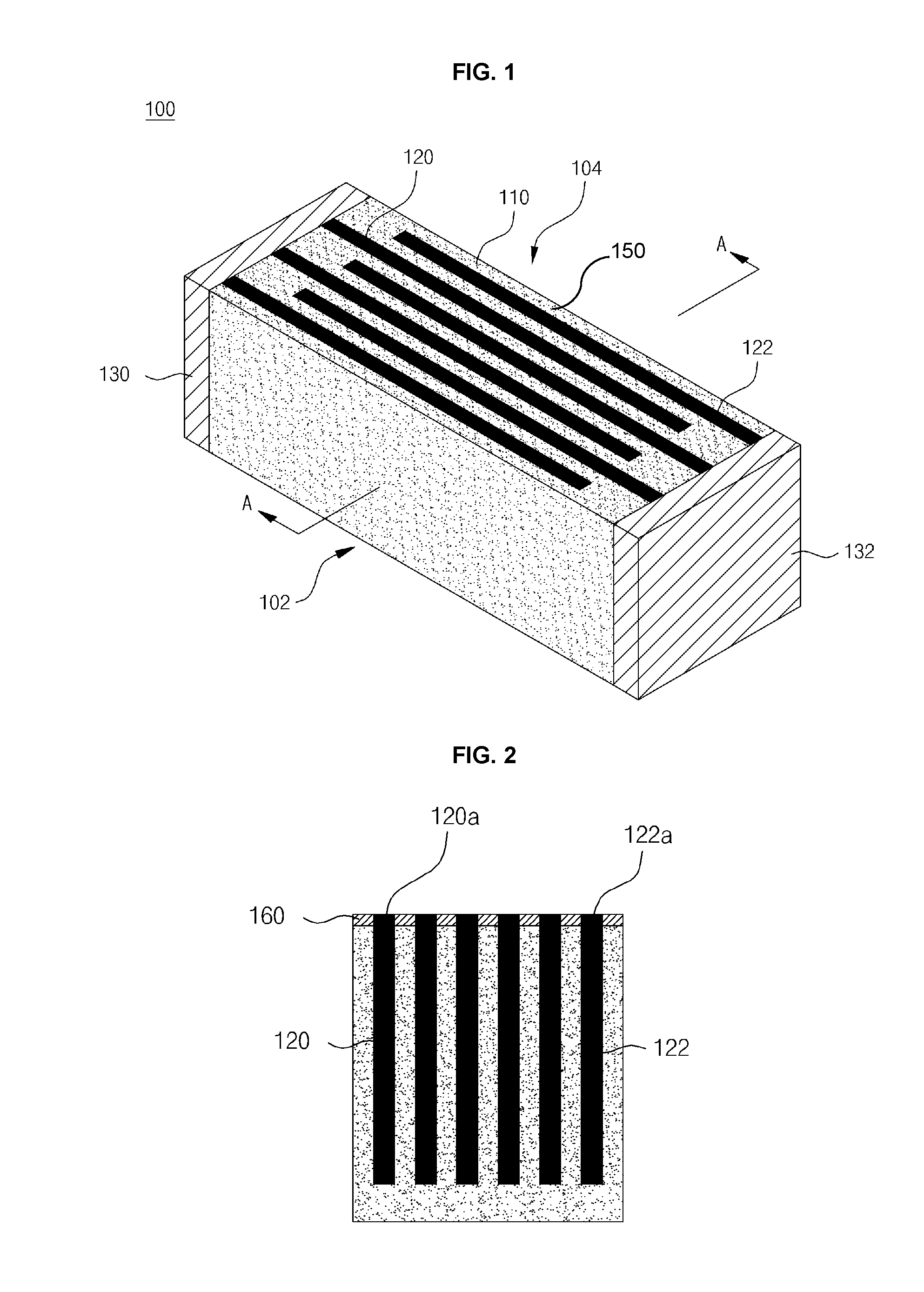
[0048]FIG. 1 is a view of a sensor 100 according to a first embodiment of the present invention.
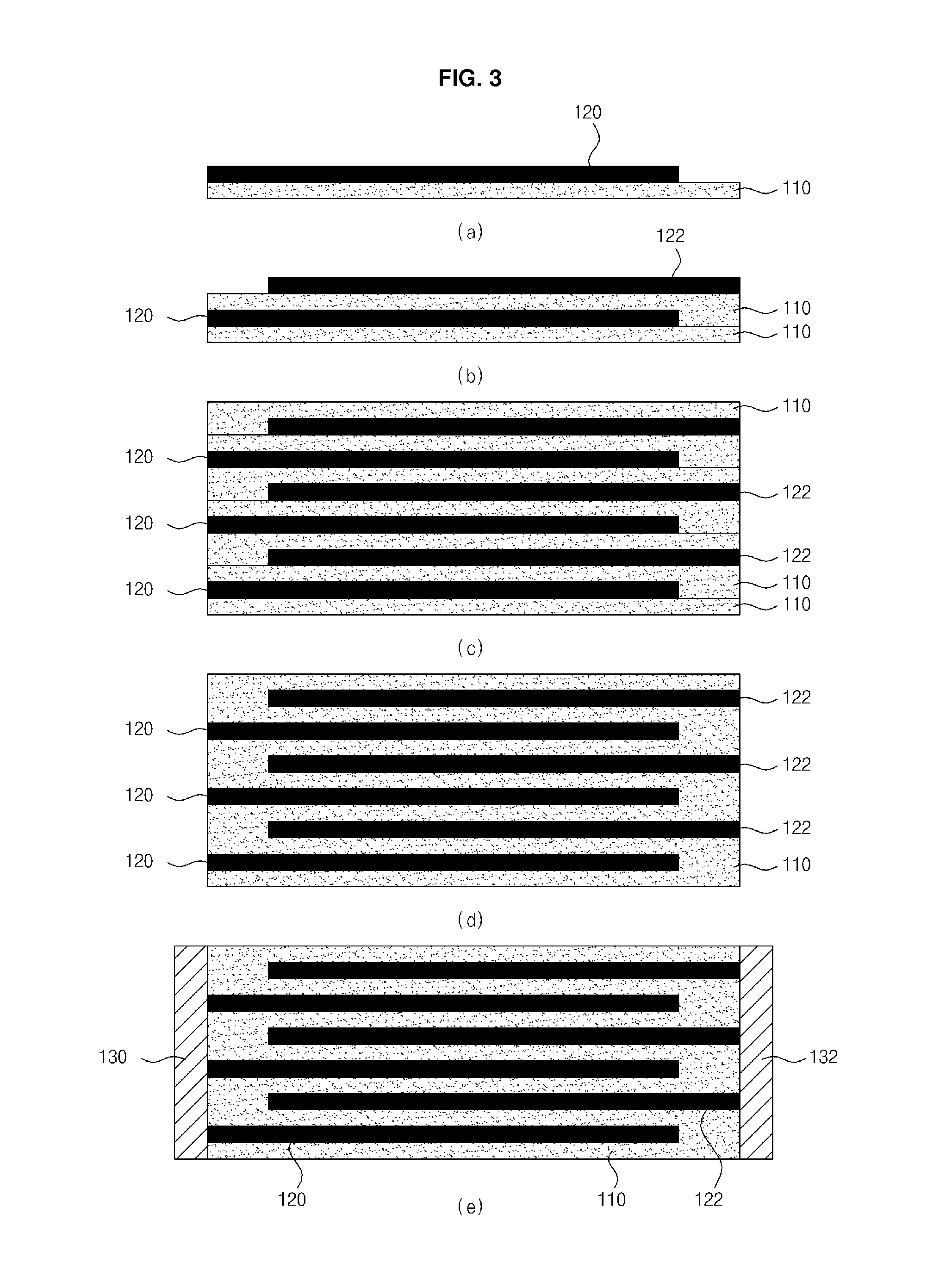
[0049]The sensor 100 includes a sensing stack 102 in which conductive layers 120 and 122 are stacked and embedded with a separation layer 110 therebetween and electrode terminals 130 and 120 respectively electrically connected to the conductive layers 120 and 122 and are disposed on side surfaces of the sensing stack 102. The conductive layers 120 and 122 may be exposed to at least one side surface of the sensing stack 102 except for the side surfaces on which the electrode terminals 130 and 132 are disposed, thereby defining a sensing surface 104.
[0050]The conductive layer 120 is exposed to only one side surface of the sensing stack 102 and electrically connected to the electrode terminal 130 to constitute one sensing electrode of the sensor 100, and the conductive layer 122 is exposed to only an opposite side surface of the sensing stack 102 and electrically connected to the electr...
second embodiment
[0087
[0088]FIG. 5 is a view of a sensor 200 according to another embodiment of the present invention.
[0089]A plurality of conductive layers 220 and 222 are embedded within one sensing stack 202 in a state where the conductive layers 220 and 222 are separated from each other by a separation layer 210. Also, a plurality of sub electrode terminals 230, 240, 250, 232, 242, and 252 are disposed on electrode terminal installation surfaces to constitute independent sensors 200a, 200b, and 200c.
[0090]The sub electrode terminals 230, 240, and 250 disposed on one side surface and the sub electrode terminals 232, 242, and 252 disposed on an opposite side surface are electrically separated from each other. In this embodiment, the conductive layers 220 and 222 having numbers different from each other are connected to each other. For example, one conductive layer may be connected to each of the sub electrode terminals 230 and 232, and two conductive layers may be connected to each of the sub ele...
third embodiment
[0094
[0095]FIG. 6 is a view of a sensor 300 according to further another embodiment of the present invention.
[0096]A plurality of conductive layers 320 and 322 are alternately arranged and embedded within one sensing stack 302 with a separation layer 310 therebetween. The conductive layer 320 has an end exposed to only one side surface and thus is electrically connected to an electrode terminal 330 disposed on the side surface. The conductive layer 322 has an end exposed to only an opposite side surface and thus is electrically connected to an electrode terminal 332 disposed on the opposite side surface.
[0097]An edge of one side of each of the plurality of conductive layers 320 and 322 is exposed to one side surface of the sensing stack 302 except for the side surface on which the electrode terminals 330 and 332 are disposed to form a sensing surface 304. A slot 340 is formed in the sensing surface 304 over an overall region in a stacked direction of the conductive layers 320 and 32...
PUM
| Property | Measurement | Unit |
|---|---|---|
| conductive | aaaaa | aaaaa |
| width | aaaaa | aaaaa |
| lengths | aaaaa | aaaaa |
Abstract
Description
Claims
Application Information
 - R&D
- Intellectual Property
- Life Sciences
- Materials
- Tech Scout
- Unparalleled Data Quality
- Higher Quality Content
- 60% Fewer Hallucinations
Browse by: Latest US Patents, China's latest patents, Technical Efficacy Thesaurus, Application Domain, Technology Topic, Popular Technical Reports.
© 2025 PatSnap. All rights reserved.Legal|Privacy policy|Modern Slavery Act Transparency Statement|Sitemap|About US| Contact US: help@patsnap.com