Supercharge Your Innovation With Domain-Expert AI Agents!

Fabrication methods for multi-layer semiconductor structures

a technology of semiconductor structure and fabrication method, which is applied in the manufacturing of semiconductor/solid-state devices, basic electric elements, electric devices, etc., can solve the problems of increasing complexity and cos

Active Publication Date: 2016-11-22
ALSEPHINA INNOVATIONS INC
View PDF3 Cites 0 Cited by
  • Summary
  • Abstract
  • Description
  • Claims
  • Application Information

AI Technical Summary

Benefits of technology

This approach simplifies the fabrication process by eliminating the need for multiple masking steps, reduces fabrication complexity, and enables precise control of threshold voltages for both p-type and n-type transistors, improving yield and reducing costs.

Problems solved by technology

For example, forming p-type transistors and n-type transistors with matched threshold voltages can require the use of multiple different gate structure formation processes or work function layers, thereby increasing complexity and costs.

Method used


Image

  • Fabrication methods for multi-layer semiconductor structures
  • Fabrication methods for multi-layer semiconductor structures
  • Fabrication methods for multi-layer semiconductor structures

Examples


Embodiment Construction

[0022]Aspects of the present invention and certain features, advantages, and details thereof, are explained more fully below with reference to the non-limiting examples illustrated in the accompanying drawings. Descriptions of well-known materials, fabrication tools, processing techniques, etc., are omitted so as not to unnecessarily obscure the invention in detail. It should be understood, however, that the detailed description and the specific examples, while indicating aspects of the invention, are given by way of illustration only, and not by way of limitation. Various substitutions, modifications, additions, and / or arrangements, within the spirit and / or scope of the underlying inventive concepts will be apparent to those skilled in the art from this disclosure.

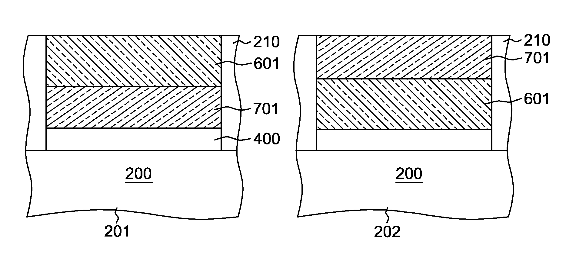
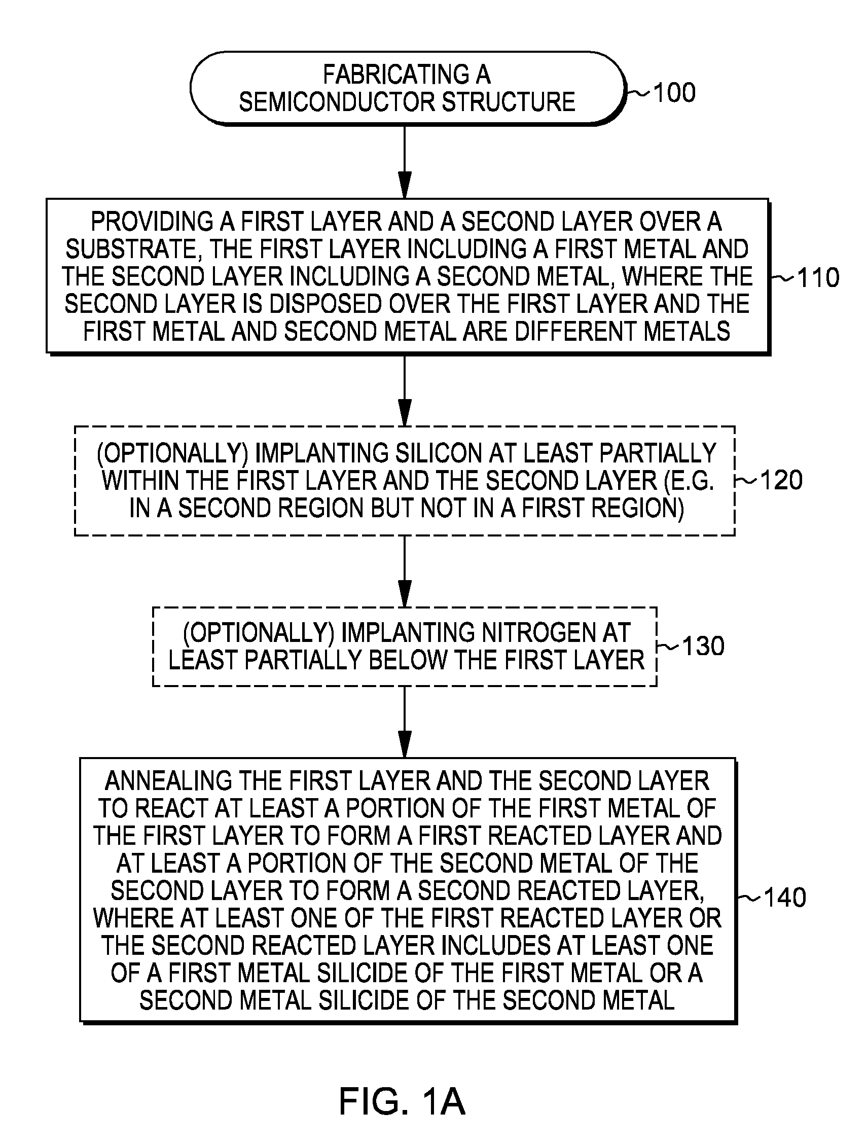
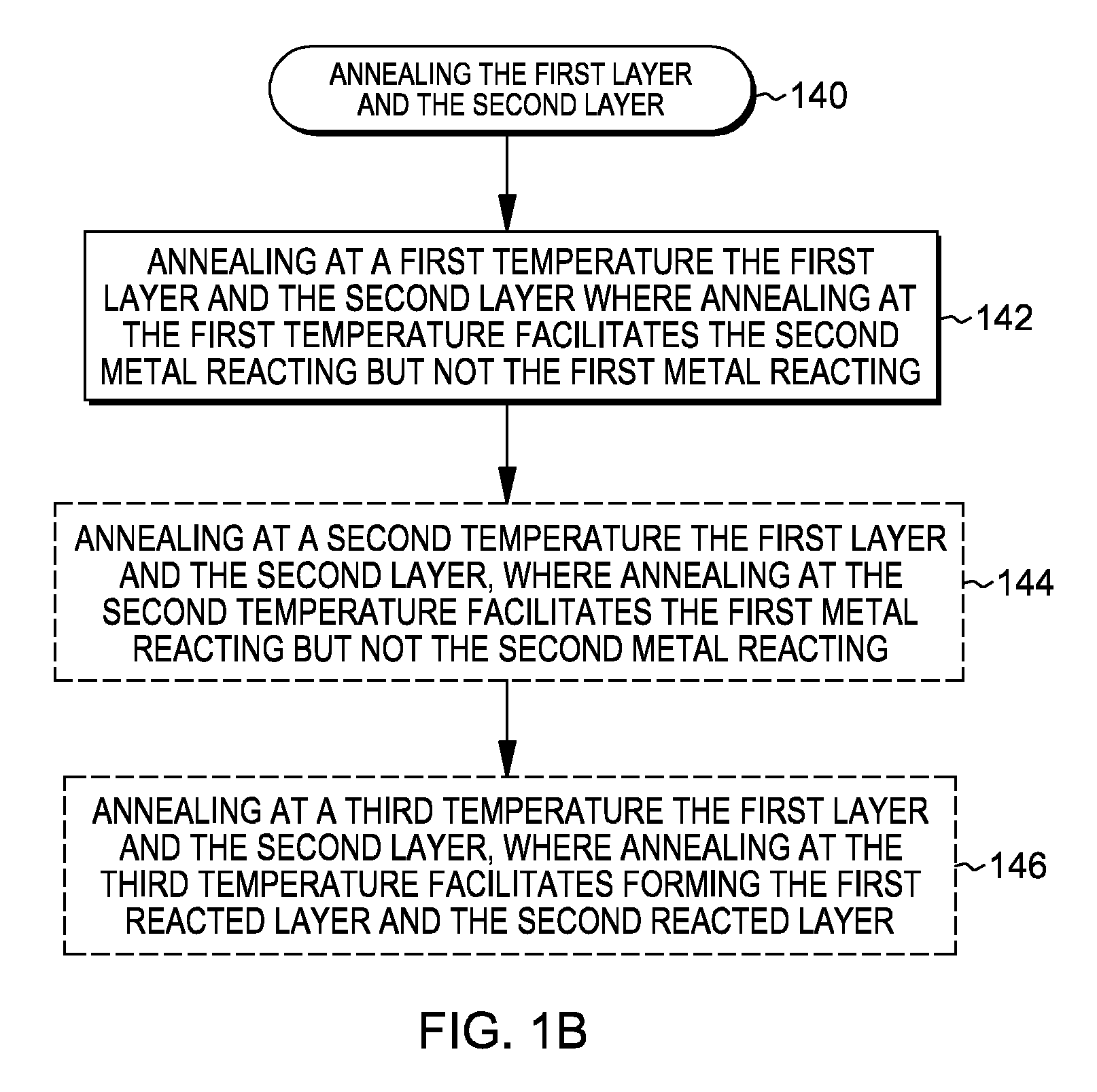
[0023]The present disclosure provides, in part, fabrication methods for multi-layer semiconductor structures. During the fabrication of integrated circuits, different processes and / or materials can be required for p-type ...


PUM

PropertyMeasurementUnit
thickaaaaaaaaaa
thicknessaaaaaaaaaa
lengthaaaaaaaaaa

Abstract

Methods are provided for fabricating multi-layer semiconductor structures. The methods include, for example: providing a first layer and a second layer over a substrate, the first layer including a first metal and the second layer including a second metal, where the second layer is disposed over the first layer and the first metal and second metal are different metals; and annealing the first layer, the second layer, and the substrate to react at least a portion of the first metal of the first layer to form a first reacted layer and at least a portion of the second metal of the second layer to form a second reacted layer, where at least one of the first reacted layer or the second reacted layer includes at least one of a first metal silicide of the first metal or a second metal silicide of the second metal.

Description

CROSS-REFERENCE TO RELATED APPLICATION[0001]This application claims the benefit of U.S. Provisional Patent Application No. 62 / 097,306, filed Dec. 29, 2014, which is hereby incorporated herein by reference in its entirety.FIELD OF THE INVENTION[0002]The present invention relates to semiconductor structures, and methods of fabricating semiconductor structures, and more particularly to fabrication methods for multi-layer semiconductor structures.BACKGROUND OF THE INVENTION[0003]Complementary metal-oxide-semiconductor (CMOS) technology continues to be an extremely important technology for the fabrication of integrated circuits. In CMOS technology, both p-type devices, such as p-type field-effect transistors, and n-type devices, such as n-type field effect transistors, are fabricated on a common semiconductor wafer.[0004]Different processes or materials can be required in the fabrication of p-type devices and n-type devices. For example, forming p-type transistors and n-type transistors ...

Claims


Application Information

Patent Timeline
Patent Type & Authority Patents(United States)
IPC IPC(8): H01L21/82H01L21/768H01L21/28H01L21/285H01L21/8234H01L21/225H01L21/283H01L21/324
CPCH01L21/823443H01L21/2253H01L21/283H01L21/285H01L21/28052H01L21/28518H01L21/324H01L21/76889H01L21/823431H01L21/82345H01L21/823821H01L21/823835H01L21/823842H01L21/28097
Inventor PATIL, SURAJ K.CHI, MIN-HWA
Owner ALSEPHINA INNOVATIONS INC
Features
  • R&D
  • Intellectual Property
  • Life Sciences
  • Materials
  • Tech Scout
  • Unparalleled Data Quality
  • Higher Quality Content
  • 60% Fewer Hallucinations
Learn More