Supercharge Your Innovation With Domain-Expert AI Agents!

Semiconductor device, heat conductor, and method for manufacturing semiconductor device

a semiconductor and heat conductor technology, applied in the direction of printed circuit aspects, basic electric elements, modification by conduction heat transfer, etc., can solve the problems of affecting the performance of the semiconductor element, carbon nanotubes arranged in the heat transfer direction may not be able to obtain the expected heat dissipation performance,

Active Publication Date: 2017-07-25
SHINKO ELECTRIC IND CO LTD
View PDF13 Cites 1 Cited by
  • Summary
  • Abstract
  • Description
  • Claims
  • Application Information

AI Technical Summary

Benefits of technology

This configuration improves heat dissipation efficiency by reducing thermal resistance and allowing for efficient heat transfer from the semiconductor element to the heat dissipation plate, enhancing the overall performance of semiconductor devices.

Problems solved by technology

This adversely affects the performance of the semiconductor element.
Thus, the carbon nanotubes arranged in the heat transfer direction may not be able to obtain the expected heat dissipation performance.

Method used


Image

  • Semiconductor device, heat conductor, and method for manufacturing semiconductor device
  • Semiconductor device, heat conductor, and method for manufacturing semiconductor device
  • Semiconductor device, heat conductor, and method for manufacturing semiconductor device

Examples


Embodiment Construction

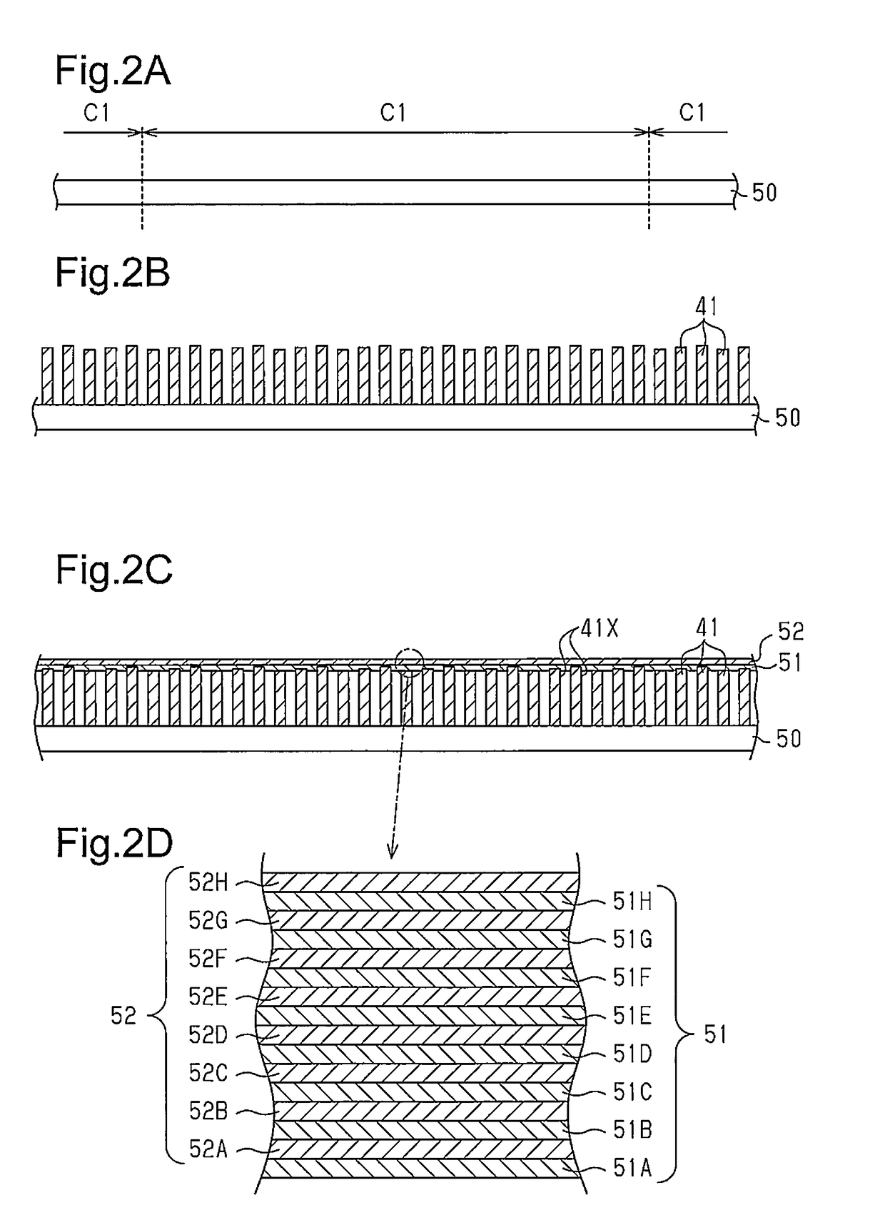
[0018]In the drawings, elements are illustrated for simplicity and clarity and have not necessarily been drawn to scale. To facilitate understanding in the cross-sectional views, instead of using hatching lines, components may be shaded.

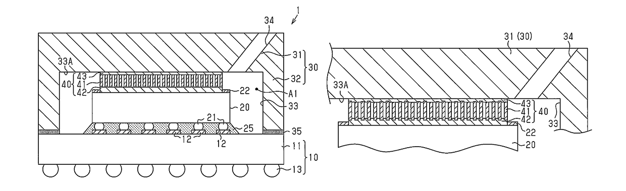
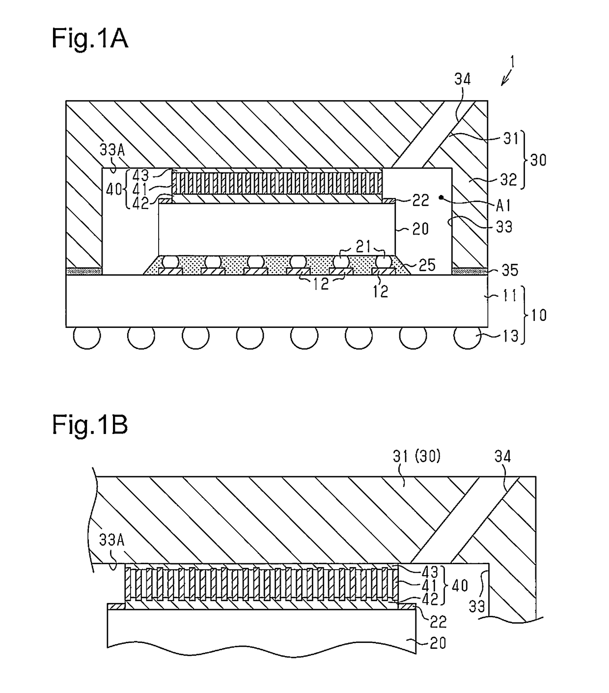
[0019]The structure of the semiconductor device 1 will now be described.

[0020]Referring to FIG. 1A, a semiconductor device 1 includes a ball grid array (BGA) wiring substrate 10, a semiconductor element 20 mounted on the upper surface of the wiring substrate 10, a heat dissipation plate 30 mounted on the upper surface of the wiring substrate 10, and a heat conductor 40 thermally coupling the semiconductor element 20 and the heat dissipation plate 30.

[0021]The wiring substrate 10 includes a substrate body 11, connection pads 12, and solder balls 13. The substrate body 11 only needs to have a structure in which the connection pads 12 and the solder balls 13 are electrically connected through the interior of the substrate body 11. Thus, wiring layers ma...


PUM


Abstract

A semiconductor device includes a wiring substrate, a semiconductor element mounted on the wiring substrate, and a heat dissipation component arranged on the wiring substrate. The heat dissipation component includes a cavity that accommodates the semiconductor element and includes an inner surface opposing the wiring substrate. The semiconductor element is located between the inner surface of the cavity and the wiring substrate. A heat conductor is bonded to the semiconductor element and to the inner surface of the cavity. The heat conductor includes linear heat conductive matters arranged between the semiconductor element and the heat dissipation component. A first alloy layer bonded to the semiconductor element covers lower ends of the heat conductive matters. The heat dissipation component includes a through hole extending through the heat dissipation component toward the heat conductor from a location outside of the heat conductor in a plan view.

Description

CROSS-REFERENCE TO RELATED APPLICATIONS[0001]This application is based upon and claims the benefit of priority from prior Japanese Patent Application No. 2014-097485, filed on May 9, 2014, the entire contents of which are incorporated herein by reference.BACKGROUND ART[0002]The present disclosure relates to a semiconductor device, a heat conductor, and a method for manufacturing a semiconductor device.[0003]A semiconductor element for a central processing unit (CPU), a graphics processing unit (GPU), or the like is electrically connected and fixed to a substrate in a semiconductor package. The semiconductor element becomes hot when activated. This adversely affects the performance of the semiconductor element. Thus, the temperature of the semiconductor element needs to be forcibly lowered.[0004]Japanese Laid-Open Patent Publication No. 2010-171200 describes a heat dissipation component (e.g., metal heat dissipation plate) that is arranged on a semiconductor element to release the he...

Claims


Application Information

Patent Timeline
Patent Type & Authority Patents(United States)
IPC IPC(8): H01L23/373H01L23/367H05K7/20H01L23/433
CPCH01L23/373H01L23/3675H01L23/3735H01L23/3737H01L23/433H05K7/2039H01L2224/16225H01L2224/32225H01L2224/73204H01L2224/73253H01L2924/15311H01L2924/16151H01L2924/16152H05K2201/0323H05K2201/066H01L2924/00
Inventor MURAYAMA, KEIIHARA, YOSHIHIRO
Owner SHINKO ELECTRIC IND CO LTD
Features
  • R&D
  • Intellectual Property
  • Life Sciences
  • Materials
  • Tech Scout
  • Unparalleled Data Quality
  • Higher Quality Content
  • 60% Fewer Hallucinations
Learn More