Display module encapsulating structure and preparing method thereof
a technology for encapsulating structures and display modules, applied in the field of display modules, can solve the problems of encapsulating structure being extremely susceptible to moisture and oxygen erosion in the external environment, and affecting the appearance of display modules
- Summary
- Abstract
- Description
- Claims
- Application Information
AI Technical Summary
Benefits of technology
Problems solved by technology
Method used
Image

Examples
embodiment 1
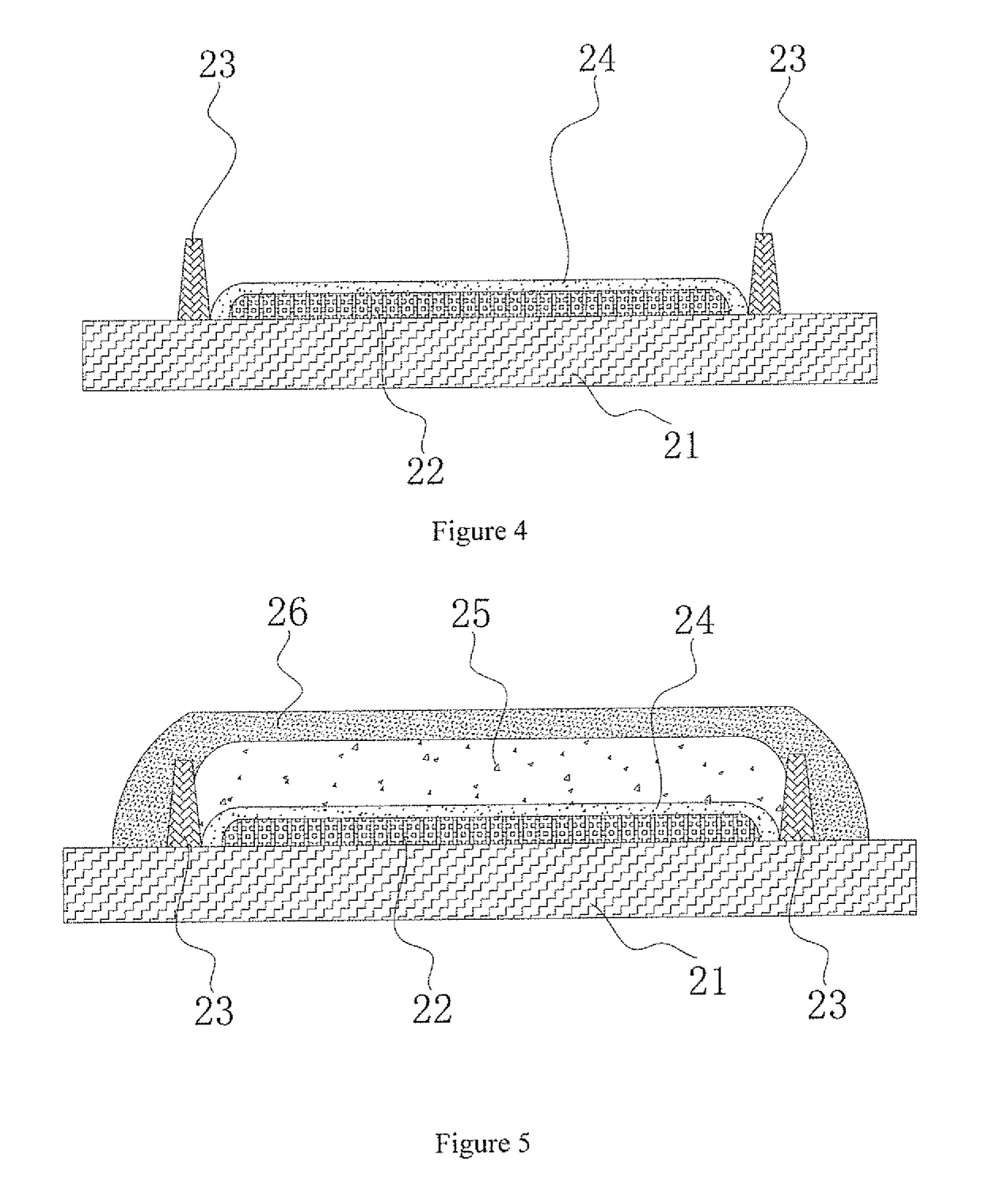
[0066]FIGS. 2 to 7 show flow charts of the processes of preparing the display module encapsulating structure in an embodiment of the present application. As shown in FIGS. 2 to 5, the application provides a method for preparing display module encapsulating structure, comprising the following steps:
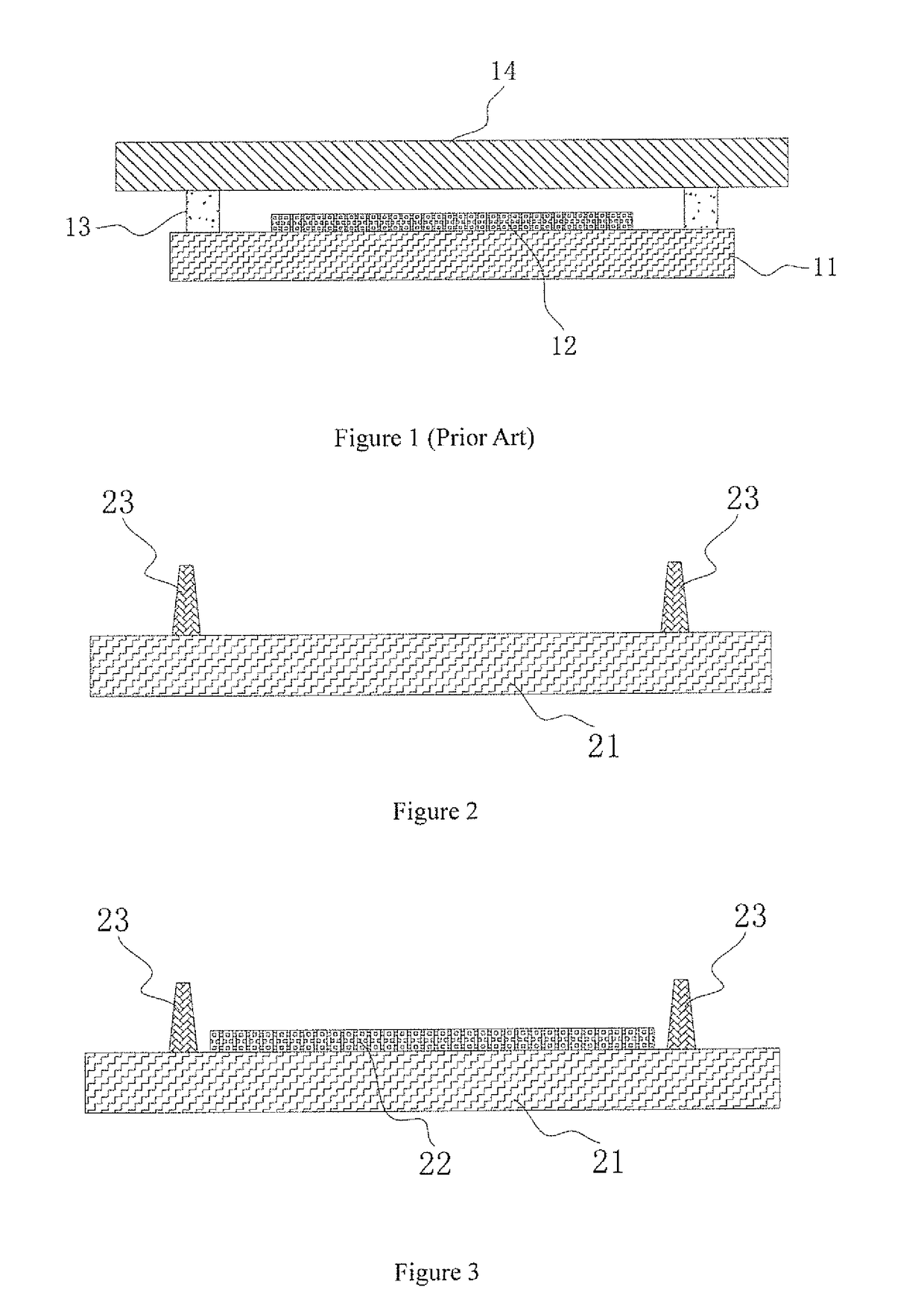
[0067]Firstly, as shown in FIG. 1, perform an array process for the display devices on the basis of a substrate (such as Low Temperature Poly Silicon-LTPS substrate) to form the array substrate 21; the above array substrate 21 can be provided with a display area and a non-display area adjacent to the display area. The array substrate 21 of the display area is mainly used for the adhesion and the preparation of the display devices; moreover, a thin film transistor display circuit could be laid out on or in the array substrate 21 to drive the display module that would be prepared subsequently.
[0068]Additionally, during the array process, the raised features 23 are formed on the surface of th...
embodiment 2
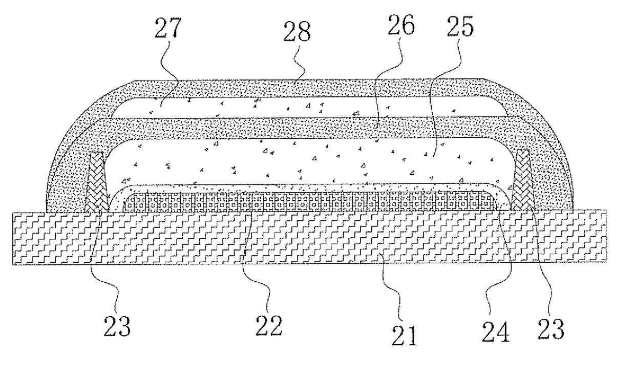
[0087]On the basis of the above embodiment 1, as shown in FIG. 7, this embodiment provides a display module encapsulating structure, said display module encapsulating structure could be used to prepare various kinds of display devices (such as OLED display device), the above display module encapsulating structure comprises:
[0088]an array substrate 21, could be a substrate to which an array process has been performed, may include but not limited to LTPS substrate, etc.; said array substrate 21 has a front surface (namely the top surface, as shown in FIG. 5) and a bottom surface opposite to the top surface (namely the bottom surface, as shown in FIGS. 5 and 6); the material of the substrate can be glass. A rigid substrate or a flexible substrate could also be used to form the array substrate 21. The array substrate 21, in or on which device structures, such as a driving circuit, used for driving the display module to emit light, could be arranged.
[0089]Additionally, the array substrat...
PUM
| Property | Measurement | Unit |
|---|---|---|
| thickness | aaaaa | aaaaa |
| thickness | aaaaa | aaaaa |
| thickness | aaaaa | aaaaa |
Abstract
Description
Claims
Application Information
 - R&D
- Intellectual Property
- Life Sciences
- Materials
- Tech Scout
- Unparalleled Data Quality
- Higher Quality Content
- 60% Fewer Hallucinations
Browse by: Latest US Patents, China's latest patents, Technical Efficacy Thesaurus, Application Domain, Technology Topic, Popular Technical Reports.
© 2025 PatSnap. All rights reserved.Legal|Privacy policy|Modern Slavery Act Transparency Statement|Sitemap|About US| Contact US: help@patsnap.com