Check patentability & draft patents in minutes with Patsnap Eureka AI!

Semiconductor device

a technology of semiconductors and auxiliary emitters, applied in the direction of electronic switching, power conversion systems, pulse techniques, etc., can solve the problems of auxiliary emitter lines with a small current carrying capacity may burn out with a heavy current, and complicated wiring, etc., to prevent current imbalance in switching operation, high current carrying capacity, and low resistance

Active Publication Date: 2017-08-01
FUJI ELECTRIC CO LTD
View PDF8 Cites 0 Cited by
  • Summary
  • Abstract
  • Description
  • Claims
  • Application Information

AI Technical Summary

Benefits of technology

The present invention aims to address the problem of potential difference in the auxiliary emitter line, which can lead to current imbalance and switching loss in conventional semiconductor devices. The invention provides a semiconductor device with a high current carrying capacity and low resistance in parallel to the base potential line between the parallel-connected switching circuits. This prevents current imbalance and minimizes switching loss in the semiconductor device.

Problems solved by technology

In the construction of the inverter circuit, the modules are prepared separately and then assembled together, leading to complicated wiring.
In the construction of parallel-connection of series-connected circuits, imbalance of operation of corresponding IGBT chips generates a potential difference between both ends of the auxiliary emitter line, which may destroy the auxiliary emitter line by abnormal current.
In addition, the auxiliary emitter line 161 with a small current carrying capacity may burn out with a heavy current.
As a consequence, even when imbalance in characteristics exists among the switching elements constructing the switching circuits connected in parallel, heavy current does not flow through the base potential line.

Method used


Image

  • Semiconductor device
  • Semiconductor device
  • Semiconductor device

Examples


third embodiment

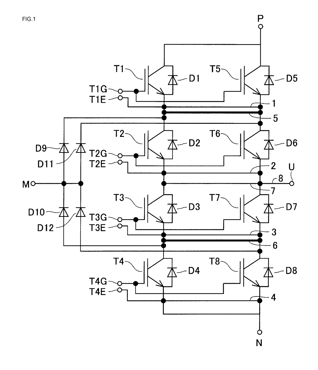
[0054]FIG. 5 is a circuit diagram of a three-level inverter circuit that is a semiconductor device according to the present invention. The components in FIG. 5 similar to those in FIG. 1 are given the same symbols.

[0055]This three-level inverter circuit that is a semiconductor device according to a third embodiment of the present invention is different from the three-level inverter circuit that is a semiconductor device according to the first embodiment in that the three-level inverter circuit of the third embodiment comprises three parallel-connected switching circuits while the three-level inverter circuit of the first embodiment comprises two parallel-connected switching circuits.

[0056]This three-level inverter circuit is composed of first, second and third switching circuits, each being a three-level inverter. The first switching circuit comprises four IGBT chips T1, T2, T3 and T4 connected in series; four free-wheeling diodes D1, D2, D3 and D4; and two clamping diodes D9 and D1...

fourth embodiment

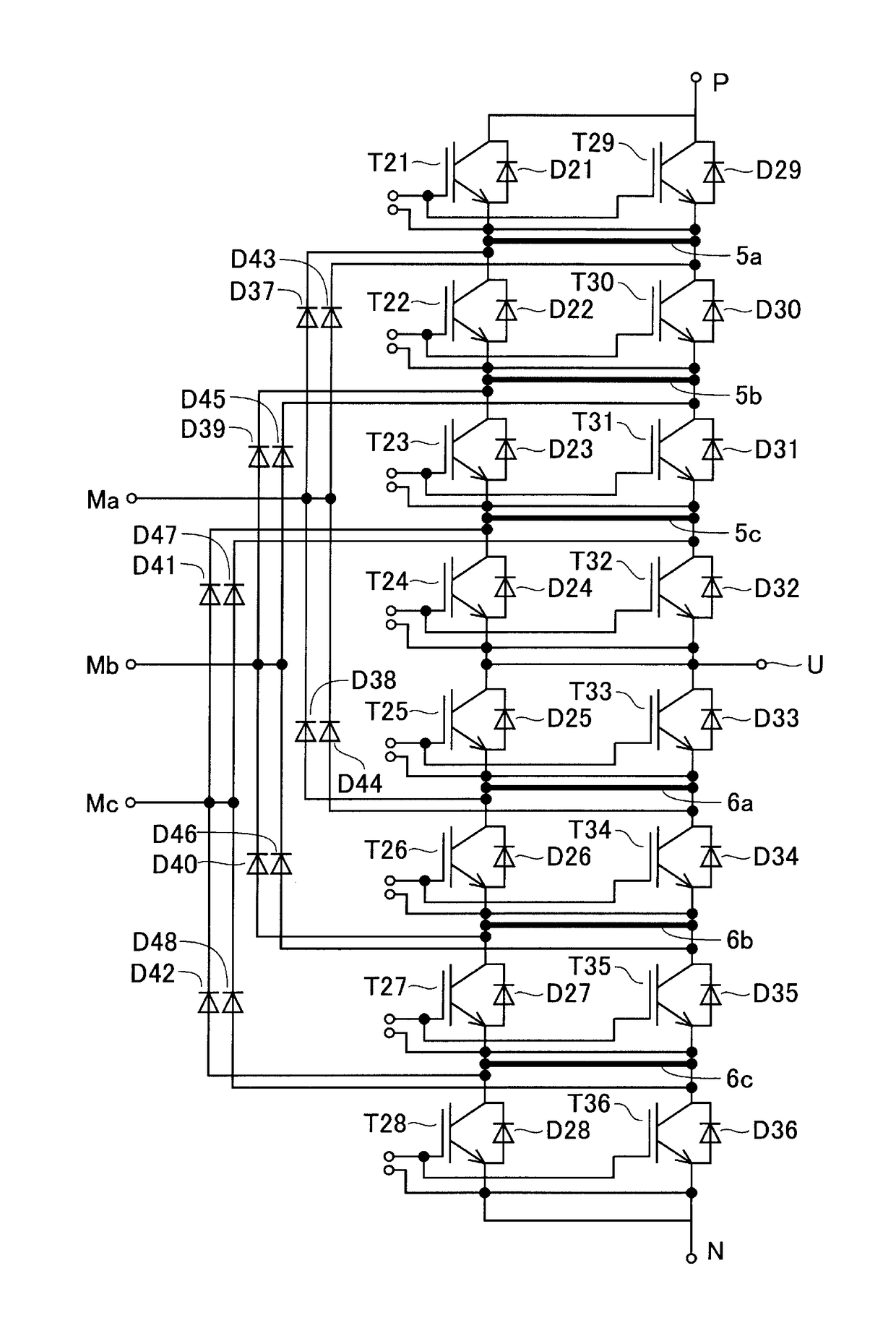
[0059]FIG. 6 is a circuit diagram of a five-level inverter circuit that is a semiconductor device according to the present invention. The components in FIG. 6 similar to those in FIG. 1 are given the same symbols.

[0060]This five-level inverter circuit that is a semiconductor device according to a fourth embodiment is composed of first and second switching circuits connected in parallel, each switching circuit being a five-level inverter. The first switching circuit comprises: eight IGBT chips T21 through T28 connected in series; eight free-wheeling diodes D21 through 28; and six clamping diodes D37 through D42. The second switching circuit comprises: eight IGBT chips T29 through T36 connected in series; eight free-wheeling diodes D29 through D36; and six clamping diodes D43 through D48.

[0061]The node between the clamping diodes D37 and D38 and the node between the clamping diodes D43 and D44 are connected to a middle potential terminal Ma. The node between the clamping diodes D39 an...


PUM


Abstract

A semiconductor device, according to one possible configuration, includes switching circuits, each switching circuit comprising IGBT chips connected in series and clamping diodes. The semiconductor device also includes a first and a second wiring line and auxiliary emitter lines. The first wiring line and a first auxiliary emitter line connect the emitter terminals of IGBT chips of the first and second switching circuits. The second wiring line and another auxiliary emitter line connect the emitter terminals of the third IGBT chips of the first and second switching circuits. The wiring lines have a large current carrying capacity and a lower resistance value than their respectively connected auxiliary emitter line.

Description

CROSS-REFERENCE TO RELATED APPLICATIONS[0001]This application is based on, and claims priority to, Japanese Patent Application No. 2014-183091, filed on Sep. 9, 2014, the content of which is incorporated herein by reference.BACKGROUND[0002]1. Field[0003]The present disclosure relates to a semiconductor device, in particular to a semiconductor device that is a power conversion module accommodating a plurality of switching elements connected in series in a package and connecting plural sets of the plurality of series-connected switching elements in parallel to increase current carrying capacity of the semiconductor device.[0004]2. Description of Related Art[0005]Semiconductor devices for power conversion often use insulated gate bipolar transistors (IGBTs), which are power switching elements exhibiting excellent operation performances in high voltage, heavy current and high speed switching. A semiconductor device having a multilevel inverter circuit is known to meet the requirements f...

Claims


Application Information

Patent Timeline
Patent Type & Authority Patents(United States)
IPC IPC(8): H03K17/567H02M1/088H02M7/487H02M7/497H02M1/00
CPCH03K17/567H02M1/088H02M7/487H02M7/497H01L2224/48091H01L2924/00014H01L2224/0603H01L2224/4903H01L2924/19107H01L2224/48472H01L2224/49113
Inventor ICHIKAWA, HIROAKI
Owner FUJI ELECTRIC CO LTD
Features
  • R&D
  • Intellectual Property
  • Life Sciences
  • Materials
  • Tech Scout
  • Unparalleled Data Quality
  • Higher Quality Content
  • 60% Fewer Hallucinations
Learn More