Supercharge Your Innovation With Domain-Expert AI Agents!

Methods of forming CIGS films

a technology of cigs and film, applied in the field of forming cigs films, can solve the problems of low bandgap and low open-circuit voltage, poor microstructure of absorber layer, and problem of back conta

Active Publication Date: 2017-09-19
ALLIANCE FOR SUSTAINABLE ENERGY
View PDF4 Cites 0 Cited by
  • Summary
  • Abstract
  • Description
  • Claims
  • Application Information

AI Technical Summary

Benefits of technology

The method results in CIGS films with improved microstructure, increased grain size, reduced voids, and enhanced photovoltaic device efficiency, achieving efficiencies of at least 14% with optimized precursor parameters and selenization conditions.

Problems solved by technology

However, as shown in FIG. 1, this method produces a CIGS absorber layer with a steep Ga gradient having low levels of Ga at the front of the CIGS absorber layer, which causes a low bandgap and a low open-circuit voltage (Voc).
Further, as shown by the cross-sectional scanning electron microscopy (SEM) image of the CIGS absorber layer in FIG. 2, this absorber layer suffers from a poor microstructure having voids, as well as problematic back contacts.
Despite efforts to homogenize the Ga distribution within the absorber layer, the efficiency of the resulting photovoltaic devices incorporating these CIGS films remains low.

Method used


Image

  • Methods of forming CIGS films
  • Methods of forming CIGS films
  • Methods of forming CIGS films

Examples


Embodiment Construction

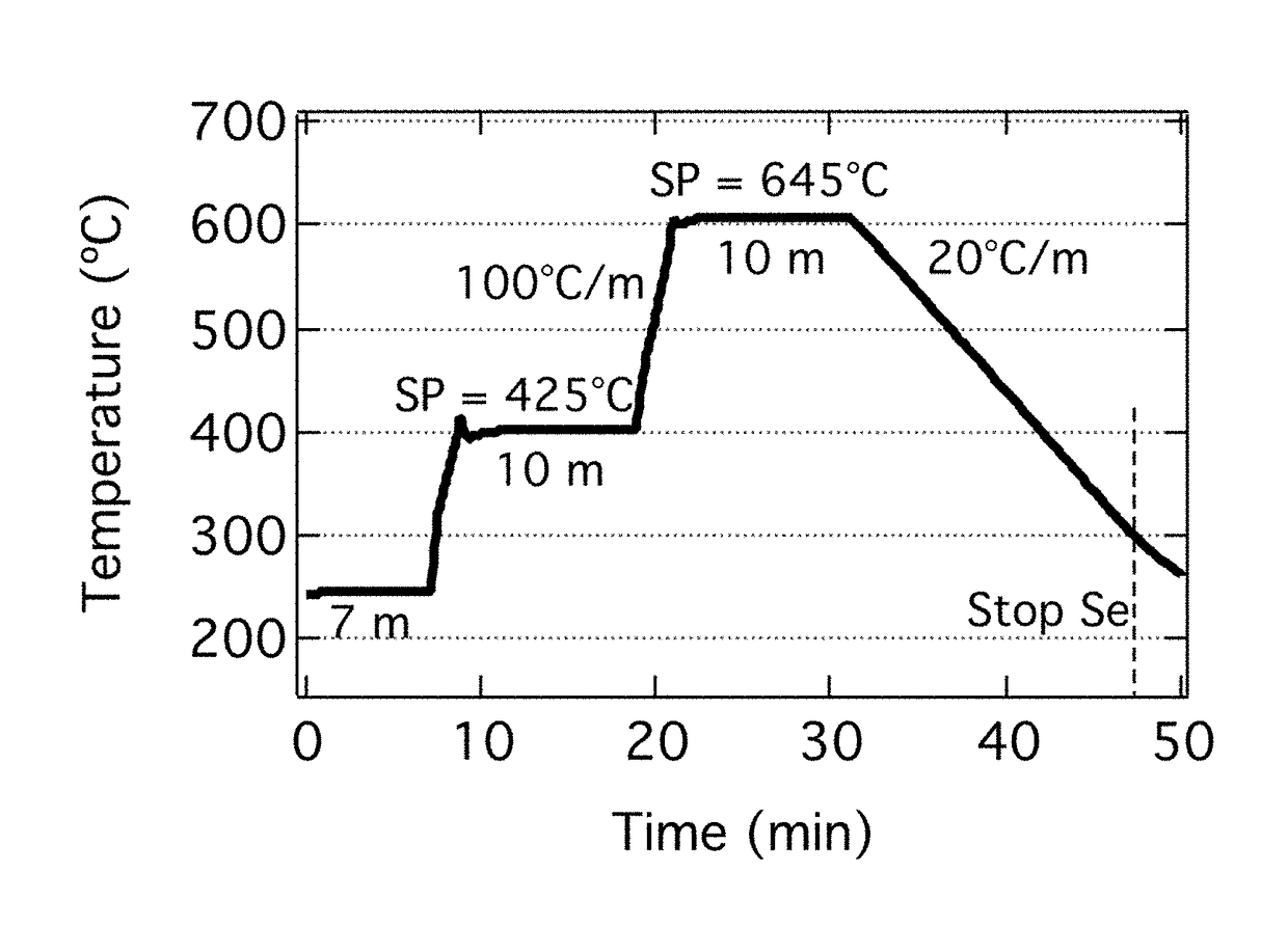
[0033]Exemplary embodiments of the present invention provide methods of forming CIGS films. The method begins with a precursor step, in which Cu, In, Ga, Se, and Sb are simultaneously evaporated onto a substrate. For example, the elements may be evaporated from tungsten boats. The substrate may be made of any suitable material, such as glass, metal foil, or a polyimide sheet, and may be coated with a back contact material, such as Mo. During the precursor step, the substrate may be maintained at a first temperature during a first time period. For example, the substrate may be maintained below approximately 350° C. while the precursors are deposited onto the substrate. After the precursor step, a selenization step is performed to produce a CIGS film. During the selenization step, elemental Se is evaporated over the substrate onto which the precursors have been deposited. In some exemplary embodiments of the present invention, the Sb may incorporated into the CIGS film as a dopant.

[00...


PUM

PropertyMeasurementUnit
temperatureaaaaaaaaaa

Abstract

Methods for forming CIGS films are provided. According to an aspect of the invention, a method of forming a CIGS film includes a precursor step, which includes simultaneously evaporating Cu, In, Ga, Se, and Sb onto a substrate. The Se is incident on the substrate at a rate of at least 20 Å / s. The method also includes a selenization step, which includes evaporating Se over the substrate after the precursor step.

Description

CROSS-REFERENCE TO RELATED APPLICATIONS[0001]This application claims priority under 35 U.S.C. §119 to U.S. Provisional Patent Application No. 62 / 174,135, filed on Jun. 11, 2015, the contents of which are hereby incorporated by reference in their entirety.CONTRACTUAL ORIGIN[0002]The United States Government has rights in this invention under Contract No. DEAC36-08GO28308 between the United States Department of Energy and the Alliance for Sustainable Energy, LLC, the Manager and Operator of the National Renewable Energy Laboratory.BACKGROUND OF THE INVENTION[0003]Photovoltaic devices that use Cu(In, Ga)Se2 (CIGS) as an absorber layer have improved in recent years, and have the potential to achieve even higher efficiencies. One related art method of forming CIGS films involves sputtering metals from Cu, Ga, and In targets, and converting these precursors into CIGS films by reacting them with Se vapor or H2Se / H2S. However, as shown in FIG. 1, this method produces a CIGS absorber layer w...

Claims


Application Information

Patent Timeline
Patent Type & Authority Patents(United States)
IPC IPC(8): H01L21/02H01L31/032
CPCH01L21/02614H01L21/02568H01L21/02631H01L31/0322Y02E10/50Y02P70/521Y02E10/541Y02P70/50
Inventor MANSFIELD, LORELLERAMANATHAN, KANNAN
Owner ALLIANCE FOR SUSTAINABLE ENERGY
Features
  • R&D
  • Intellectual Property
  • Life Sciences
  • Materials
  • Tech Scout
  • Unparalleled Data Quality
  • Higher Quality Content
  • 60% Fewer Hallucinations
Learn More