Achieving Compact Design with Wafer-Level Optics in Embedded Systems
APR 9, 20269 MIN READ
Generate Your Research Report Instantly with AI Agent
PatSnap Eureka helps you evaluate technical feasibility & market potential.
Wafer-Level Optics Background and Miniaturization Goals
Wafer-level optics represents a paradigm shift in optical system manufacturing, where optical elements are fabricated directly on semiconductor wafers using established microfabrication processes. This technology emerged from the convergence of semiconductor manufacturing capabilities and the growing demand for miniaturized optical systems in consumer electronics, automotive sensors, and medical devices. Unlike traditional optical components that are individually manufactured and assembled, wafer-level optics enables batch production of thousands of optical elements simultaneously on a single wafer substrate.
The historical development of wafer-level optics traces back to the early 2000s when semiconductor foundries began exploring applications beyond traditional electronic circuits. Initial implementations focused on simple refractive elements such as microlenses and optical windows. The technology gained significant momentum with the proliferation of smartphone cameras, where space constraints and cost pressures drove innovation in compact optical solutions. Key technological milestones include the development of wafer-level cameras around 2008, followed by advanced multi-element optical stacks and integrated optical-electronic systems.
Current miniaturization goals in wafer-level optics are driven by the relentless pursuit of smaller, lighter, and more cost-effective embedded systems. The primary objective centers on achieving sub-millimeter optical system heights while maintaining or improving optical performance compared to conventional lens assemblies. This includes reducing the total track length of imaging systems to less than 3mm for mobile applications and achieving form factors suitable for wearable devices and Internet of Things sensors.
Performance targets encompass maintaining optical quality metrics such as modulation transfer function and distortion control within acceptable ranges despite the geometric constraints. The industry aims to achieve F-numbers below 2.0 while supporting high-resolution imaging capabilities exceeding 12 megapixels in compact form factors. Additionally, there is a strong emphasis on integrating multiple optical functions within single wafer-level packages, including autofocus mechanisms, optical image stabilization, and spectral filtering capabilities.
Manufacturing scalability represents another critical goal, with the objective of leveraging semiconductor fab infrastructure to achieve cost parity with traditional optical systems at high volumes. This includes developing processes compatible with 200mm and 300mm wafer formats and achieving yield rates exceeding 95% for commercial viability. The ultimate vision encompasses fully integrated opto-electronic systems where optical elements, image sensors, and processing circuits coexist on the same substrate, enabling unprecedented levels of miniaturization and functionality integration.
Market Demand for Compact Embedded Optical Systems
The embedded systems market is experiencing unprecedented growth driven by the proliferation of Internet of Things devices, autonomous vehicles, augmented reality applications, and advanced mobile technologies. This expansion has created substantial demand for optical components that can deliver high performance while maintaining extremely compact form factors. Traditional optical systems, with their bulky lenses and complex assemblies, are increasingly inadequate for modern embedded applications where space constraints are paramount.
Consumer electronics represent the largest segment driving this demand, particularly in smartphones, tablets, and wearable devices. The continuous push for thinner devices with enhanced camera capabilities has intensified the need for miniaturized optical solutions. Manufacturers are seeking optical systems that can provide multiple functionalities including imaging, sensing, and display projection within millimeter-scale packages.
The automotive industry presents another significant growth driver, especially with the advancement of autonomous driving technologies. Modern vehicles require numerous optical sensors for LiDAR systems, driver monitoring, gesture recognition, and advanced driver assistance systems. These applications demand robust, compact optical solutions that can withstand harsh environmental conditions while maintaining precise performance specifications.
Industrial automation and robotics sectors are increasingly adopting embedded optical systems for machine vision, quality control, and navigation applications. The trend toward smaller, more intelligent robotic systems has created demand for miniaturized optical components that can provide high-resolution imaging and accurate distance measurement capabilities.
Healthcare and medical device markets are experiencing growing demand for compact optical systems in portable diagnostic equipment, endoscopic devices, and wearable health monitors. The shift toward point-of-care testing and remote patient monitoring has accelerated the need for miniaturized optical solutions that can deliver laboratory-grade performance in portable formats.
The aerospace and defense sectors require highly reliable, compact optical systems for surveillance, communication, and navigation applications. Space constraints in satellites, drones, and portable military equipment drive the demand for wafer-level optical solutions that can withstand extreme operating conditions while maintaining exceptional performance standards.
Market growth is further accelerated by emerging applications in augmented and virtual reality systems, where compact optical engines are essential for creating immersive experiences in lightweight headsets. The gaming and entertainment industries are pushing for increasingly sophisticated optical systems that can deliver high-resolution displays and accurate motion tracking in consumer-friendly form factors.
Current State and Challenges of WLO Integration
Wafer-level optics technology has reached a significant maturity level in manufacturing processes, with established fabrication techniques enabling mass production of miniaturized optical components. Current WLO integration capabilities demonstrate successful implementation in smartphone cameras, automotive sensors, and medical devices, where space constraints demand ultra-compact optical solutions. The technology has proven effective in reducing overall system thickness by 30-50% compared to traditional lens assemblies while maintaining acceptable optical performance standards.
However, several critical challenges persist in achieving optimal WLO integration within embedded systems. Thermal management represents a primary concern, as wafer-level optical elements exhibit heightened sensitivity to temperature variations, potentially causing focal shifts and aberration changes that compromise system reliability. The coefficient of thermal expansion mismatch between optical materials and semiconductor substrates creates mechanical stress during temperature cycling, leading to potential delamination or cracking issues.
Manufacturing yield consistency remains problematic, particularly in high-volume production scenarios. Current fabrication processes struggle with maintaining uniform optical surface quality across entire wafer batches, resulting in performance variations that affect system-level specifications. The replication accuracy of micro-optical structures often falls short of theoretical requirements, especially for complex aspherical geometries and diffractive elements.
Integration complexity escalates when combining WLO components with electronic circuits and mechanical assemblies. Precise alignment tolerances, typically requiring sub-micron accuracy, present significant challenges during assembly processes. The lack of standardized packaging solutions for WLO-embedded systems creates compatibility issues across different platform architectures and manufacturing ecosystems.
Cost optimization remains a substantial barrier for widespread adoption. While wafer-level processing theoretically enables economies of scale, the specialized equipment requirements and low initial yields result in higher per-unit costs compared to conventional optical solutions. Additionally, the limited availability of qualified suppliers and specialized materials constrains market accessibility and drives up procurement expenses for embedded system manufacturers.
Quality assurance and testing methodologies for WLO-integrated systems require further development. Traditional optical testing approaches prove inadequate for evaluating wafer-level components within embedded environments, necessitating new measurement techniques and validation protocols that can assess performance under actual operating conditions while maintaining production throughput requirements.
Existing WLO Solutions for Compact Design
01 Wafer-level lens array integration and alignment techniques
This approach involves integrating multiple lens elements at the wafer level through precise alignment and bonding techniques. The method enables mass production of compact optical systems by forming lens arrays on wafer substrates and aligning them with image sensors or other optical components. Advanced alignment structures and bonding methods ensure accurate positioning between optical elements, reducing overall package size while maintaining optical performance. This technique is particularly suitable for miniaturized camera modules in mobile devices and compact imaging systems.- Wafer-level lens array integration and alignment techniques: This approach focuses on integrating multiple lens elements at the wafer level through precise alignment and bonding techniques. The method enables mass production of compact optical systems by forming lens arrays on wafer substrates and aligning them with image sensor arrays. Advanced alignment structures and bonding methods ensure accurate positioning between optical elements and sensors, reducing overall package size while maintaining optical performance.
- Stacked wafer-level optical module architecture: This technology involves stacking multiple wafer-level optical components vertically to create compact camera modules. The stacked architecture includes image sensors, lens wafers, and spacer wafers assembled in a layered configuration. This design minimizes the lateral footprint and overall height of the optical system, making it suitable for mobile devices and miniaturized imaging applications. The approach also facilitates integration of additional functional layers such as filters and apertures.
- Molded wafer-level optics with integrated optical elements: This technique utilizes molding processes to form optical elements directly on wafer substrates, enabling integration of complex lens shapes and optical surfaces. The molding approach allows for high-volume manufacturing of aspherical and freeform optical elements with reduced thickness. Multiple optical functions can be integrated into a single wafer-level component, including refractive and diffractive elements, resulting in compact optical designs with enhanced performance.
- Wafer-level packaging with embedded optical components: This method embeds optical components within wafer-level packages to achieve ultra-compact designs. The packaging approach integrates lenses, filters, and other optical elements into the package structure itself, eliminating the need for separate assembly steps. This results in reduced package height and improved optical alignment stability. The embedded components are protected by the package structure, enhancing reliability while maintaining compact dimensions.
- Hybrid wafer-level optics with active alignment systems: This approach combines wafer-level optical fabrication with active alignment mechanisms to optimize optical performance in compact designs. The system incorporates adjustment capabilities during or after assembly to compensate for manufacturing tolerances. Active alignment techniques ensure optimal focus and image quality while maintaining minimal package size. The hybrid approach balances the benefits of wafer-level manufacturing efficiency with the precision of active alignment, suitable for high-performance compact imaging systems.
02 Stacked wafer-level optical element design
This technology focuses on vertically stacking multiple wafer-level optical components to achieve compact optical designs. By stacking lens wafers, filter wafers, and sensor wafers in a vertical configuration, the lateral footprint is minimized while maintaining or enhancing optical functionality. The stacked architecture allows for integration of multiple optical functions including focusing, filtering, and light manipulation within a compact volume. Spacer structures and bonding layers between wafers ensure proper optical path lengths and mechanical stability.Expand Specific Solutions03 Wafer-level packaging with integrated optical elements
This method combines wafer-level packaging techniques with integrated optical components to create compact optical modules. The approach involves forming optical elements directly on or within the package structure, eliminating the need for separate optical component assembly. Techniques include molding lenses directly on wafer surfaces, integrating diffractive optical elements, and incorporating optical coatings at the wafer level. This integration reduces package height and simplifies assembly processes while providing environmental protection for sensitive optical and electronic components.Expand Specific Solutions04 Micro-optical element fabrication on wafer substrates
This technique involves fabricating micro-scale optical elements directly on wafer substrates using semiconductor manufacturing processes. Methods include reflow processes for forming curved lens surfaces, etching techniques for creating diffractive structures, and deposition processes for optical coatings. The wafer-level fabrication enables precise control of optical element dimensions and properties while allowing batch processing for cost-effective production. These micro-optical elements can include microlenses, beam splitters, and light redirecting structures optimized for compact optical system designs.Expand Specific Solutions05 Wafer-level optical system with reduced height profile
This design approach focuses on minimizing the overall height of wafer-level optical systems through innovative optical architectures and component arrangements. Techniques include using folded optical paths, implementing thin optical elements, and optimizing the spacing between components. The design may incorporate reflective elements or prisms to redirect light paths, allowing for reduced package thickness. Special attention is given to maintaining image quality while achieving ultra-compact form factors suitable for slim electronic devices and space-constrained applications.Expand Specific Solutions
Key Players in WLO and Embedded Systems Industry
The wafer-level optics market for embedded systems is experiencing rapid growth, driven by increasing demand for compact, high-performance optical solutions in consumer electronics, automotive, and AR/VR applications. The industry is in an expansion phase with significant market opportunities, as evidenced by major players like Apple, Samsung Electronics, and Google integrating advanced optical technologies into their devices. Technology maturity varies across segments, with established companies like Canon, Olympus, and Sony demonstrating mature imaging capabilities, while specialized firms such as Lumus, LensVector, and Jade Bird Display are pioneering next-generation solutions. Manufacturing leaders including TSMC, ASML, and Himax Technologies provide critical foundational technologies, while companies like Anteryon International and Digital Optics Corp. focus specifically on wafer-level optical innovations. The competitive landscape shows a mix of established semiconductor giants and emerging specialized optical technology providers, indicating a dynamic market with both proven solutions and cutting-edge developments converging to address the growing demand for miniaturized optical systems.
Lumus Ltd.
Technical Solution: Lumus has developed proprietary wafer-level optics technology for augmented reality displays, utilizing reflective waveguide technology that enables ultra-compact optical engines. Their approach involves manufacturing optical elements directly on semiconductor wafers, achieving thickness reductions of up to 80% compared to traditional optics while maintaining high optical performance. The company's wafer-level fabrication process integrates multiple optical functions into single substrates, enabling mass production of miniaturized optical systems for embedded applications including smart glasses and automotive head-up displays.
Strengths: Pioneering AR optics with proven miniaturization capabilities and established manufacturing processes. Weaknesses: Limited to specific AR applications with high development costs for new market segments.
Fraunhofer-Gesellschaft eV
Technical Solution: Fraunhofer institutes have developed innovative wafer-level optics manufacturing processes including micro-replication techniques, precision molding, and direct laser writing for creating complex optical microstructures. Their research focuses on scalable production methods for diffractive optical elements, micro-lens arrays, and freeform optics at the wafer scale. The organization's technologies enable cost-effective mass production of miniaturized optical components with feature sizes down to sub-micron levels, supporting applications in sensors, displays, and optical communication systems through advanced lithographic and etching processes.
Strengths: Cutting-edge research capabilities with strong fundamental technology development and extensive collaboration networks with industry partners. Weaknesses: Research-focused organization with longer technology transfer timelines and limited direct manufacturing capabilities for commercial applications.
Core Patents in Wafer-Level Optical Technologies
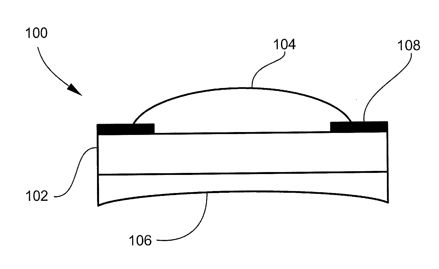
Wafer level optical elements and applications thereof
PatentInactiveUS20110002053A1
Innovation
- Wafer level optical elements are designed without a supporting substrate between optical structures, featuring coupled lens structures with an interface and integrated apertures, allowing for improved optical performance, reduced center thickness, and thermal stability through material matching of lens structures and apertures.
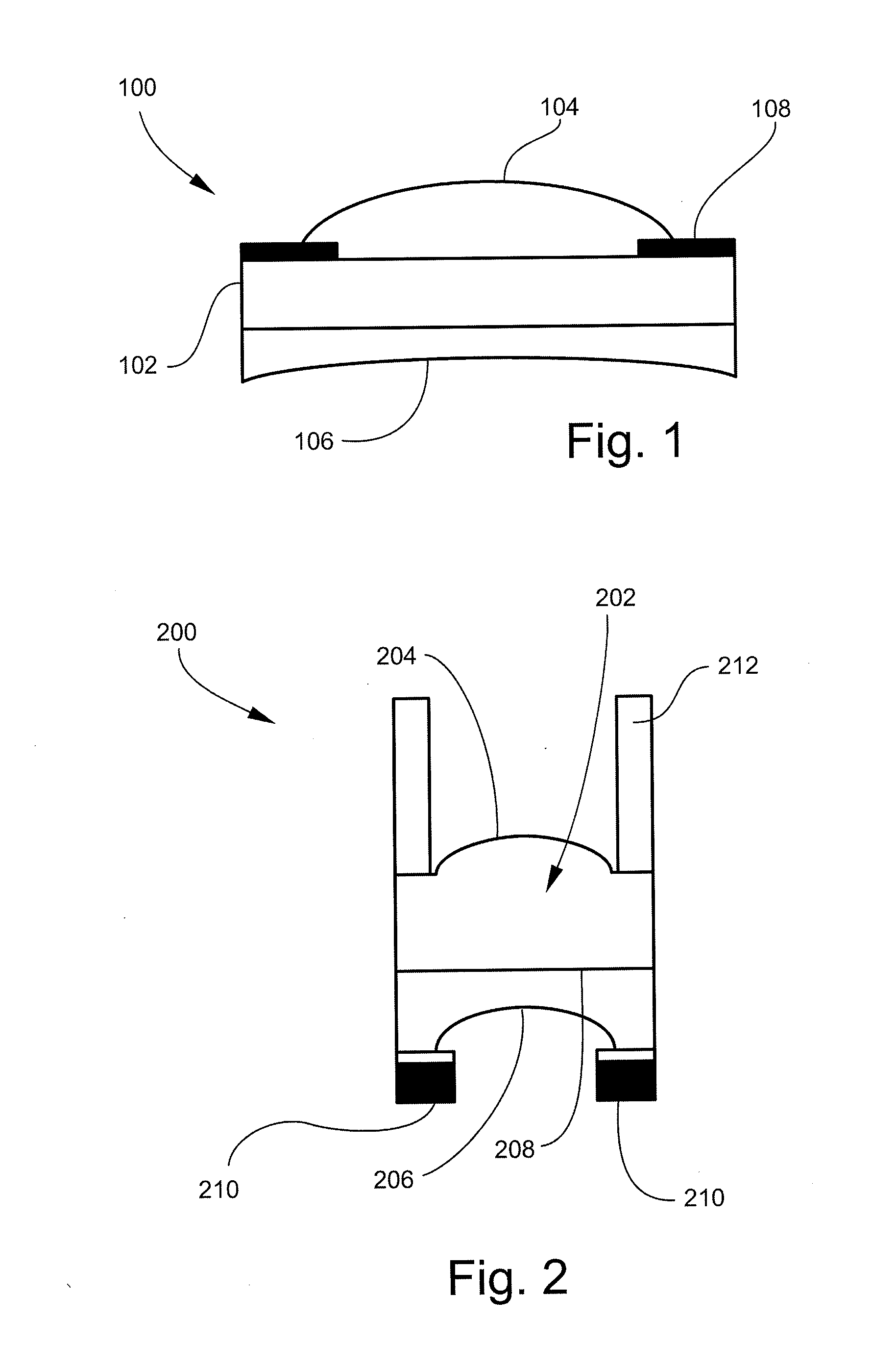

Compact three-surface wafer-level lens systems
PatentActiveUS20170307856A1
Innovation
- A compact three-surface wafer-level lens system is developed, comprising a first and second wafer-level lens, optimized for low total track length and maximum transverse extent, enabling a wide field of view while maintaining high optical performance, and manufactured using wafer-level processes compatible with reflow soldering for cost-effective production.


Manufacturing Standards for WLO Production
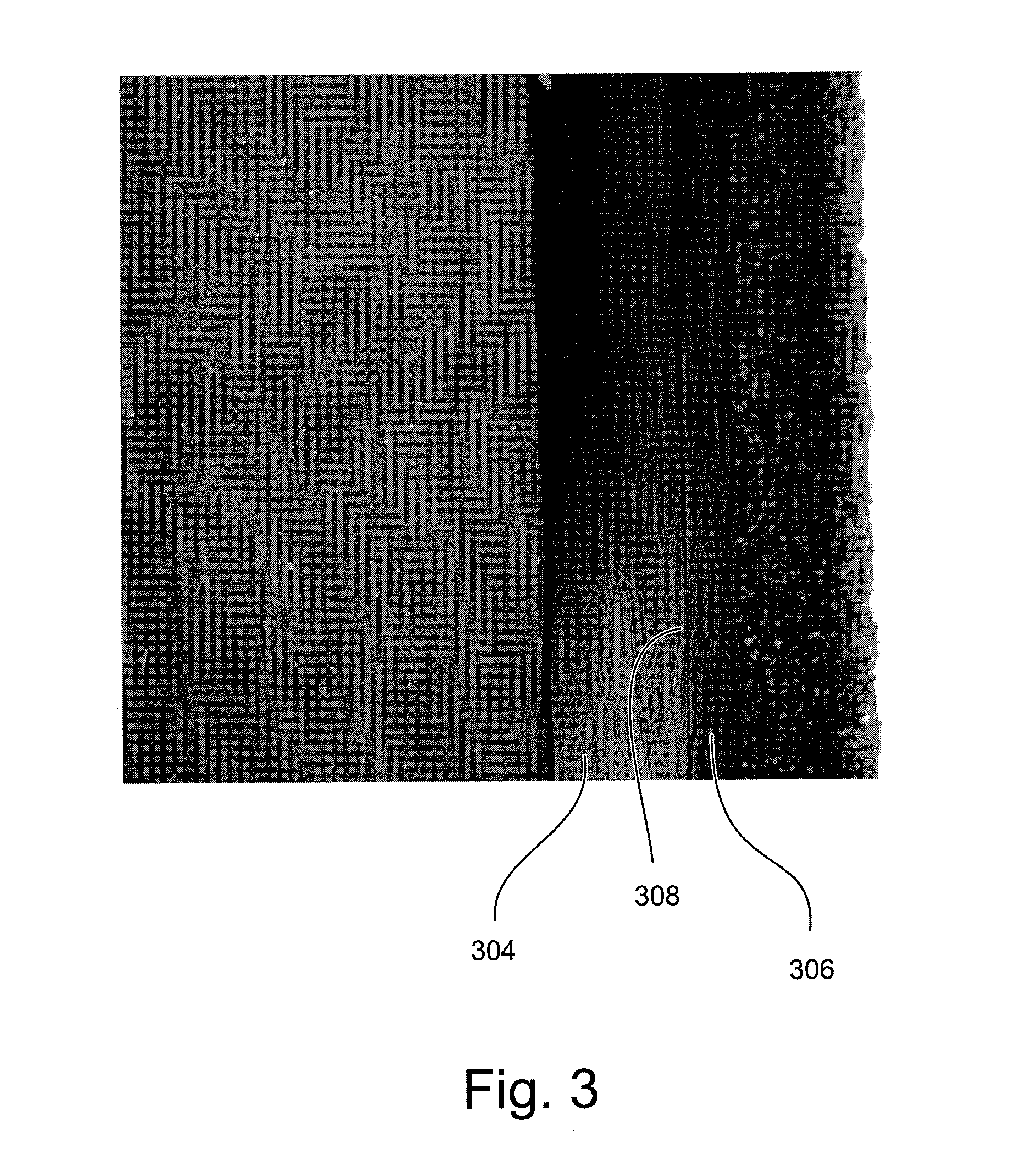
The manufacturing of wafer-level optics requires adherence to stringent standards that ensure consistent quality, performance, and reliability across production batches. Current industry standards primarily derive from semiconductor manufacturing protocols, adapted specifically for optical component fabrication. These standards encompass dimensional tolerances, surface quality specifications, and optical performance metrics that must be maintained throughout the production process.
ISO 10110 series standards serve as the foundation for optical element specifications in WLO manufacturing, defining surface form deviations, surface imperfections, and material homogeneity requirements. For wafer-level applications, these standards have been refined to accommodate the unique challenges of batch processing and miniaturization. Surface roughness specifications typically require Ra values below 1 nanometer for critical optical surfaces, while form accuracy must be maintained within λ/10 across the entire wafer surface.
Semiconductor industry standards such as SEMI specifications provide crucial guidelines for wafer handling, cleanliness protocols, and contamination control during WLO production. These standards establish requirements for cleanroom environments, typically Class 10 or better, and define particle contamination limits that directly impact optical performance. The integration of these semiconductor standards with optical manufacturing requirements creates a comprehensive framework for WLO production quality control.
Material specifications represent another critical aspect of WLO manufacturing standards. Glass wafer composition must meet strict optical property requirements, including refractive index uniformity within ±0.0001 across the wafer surface and stress birefringence levels below 2 nm/cm. These specifications ensure consistent optical performance across all individual components produced from a single wafer.
Process control standards focus on maintaining repeatability and yield optimization throughout the manufacturing sequence. Statistical process control methodologies, adapted from semiconductor fabrication, monitor critical parameters such as etch rates, deposition uniformity, and thermal processing conditions. These standards typically require Cpk values above 1.33 for critical process parameters to ensure six-sigma quality levels.
Emerging standards specifically address the unique requirements of embedded system applications, including thermal cycling specifications, mechanical shock resistance, and long-term reliability under varying environmental conditions. These application-specific standards bridge the gap between traditional optical component specifications and the demanding requirements of embedded system integration.
Thermal Management in Compact Optical Designs
Thermal management represents one of the most critical challenges in achieving compact wafer-level optical designs for embedded systems. As optical components are miniaturized and integrated at the wafer level, heat generation becomes concentrated in extremely small volumes, creating thermal hotspots that can significantly impact optical performance and system reliability. The challenge is compounded by the limited space available for traditional cooling solutions in compact embedded applications.
Heat generation in wafer-level optical systems primarily stems from active components such as laser diodes, photodetectors, and optical modulators. These components generate heat through electrical resistance, optical absorption, and quantum inefficiencies. In compact designs, the proximity of multiple heat-generating elements creates thermal coupling effects, where heat from one component affects the performance of adjacent optical elements. This thermal crosstalk can lead to wavelength drift, reduced quantum efficiency, and accelerated degradation of optical materials.
Effective thermal management strategies for compact optical designs must address both heat removal and thermal isolation. Micro-scale heat sinks fabricated using semiconductor processing techniques offer one approach, utilizing high-aspect-ratio fins and enhanced surface areas to improve heat dissipation within minimal footprints. Advanced materials such as diamond-like carbon coatings and graphene-based thermal interface materials provide superior thermal conductivity while maintaining optical transparency where required.
Thermal isolation techniques become equally important in preventing heat transfer between sensitive optical components. Micro-trenches etched into silicon substrates can create thermal barriers, while selective material deposition allows for localized thermal management. Active cooling solutions, including thermoelectric coolers integrated at the wafer level, provide precise temperature control for critical components such as laser sources and sensitive detectors.
Design optimization requires careful consideration of thermal pathways and heat distribution patterns. Computational thermal modeling enables prediction of temperature gradients and identification of optimal component placement to minimize thermal interference. The integration of temperature sensors at the wafer level allows for real-time thermal monitoring and adaptive control strategies, ensuring optimal performance across varying operating conditions and environmental temperatures.
Unlock deeper insights with PatSnap Eureka Quick Research — get a full tech report to explore trends and direct your research. Try now!
Generate Your Research Report Instantly with AI Agent
Supercharge your innovation with PatSnap Eureka AI Agent Platform!