

Achieving Superior Rectification with Schottky Diode Circuits
MAR 24, 20269 MIN READ
Generate Your Research Report Instantly with AI Agent
PatSnap Eureka helps you evaluate technical feasibility & market potential.
Schottky Diode Rectification Background and Objectives
Schottky diodes represent a fundamental advancement in semiconductor rectification technology, distinguished by their unique metal-semiconductor junction structure that eliminates the traditional p-n junction found in conventional diodes. This distinctive architecture enables significantly reduced forward voltage drop, typically ranging from 0.15V to 0.45V compared to 0.7V in standard silicon diodes, making them particularly valuable for high-efficiency power conversion applications.
The evolution of Schottky diode technology traces back to the 1930s when Walter Schottky first described the metal-semiconductor barrier phenomenon. However, practical implementation didn't emerge until the 1960s with advances in semiconductor manufacturing processes. The technology gained substantial momentum during the 1980s as switching power supplies became prevalent, driving demand for components capable of high-frequency operation with minimal power losses.
Contemporary rectification challenges in power electronics demand solutions that address multiple performance criteria simultaneously. Traditional silicon diodes suffer from significant reverse recovery time limitations, typically 25-100 nanoseconds, which creates substantial switching losses in high-frequency applications. Additionally, the higher forward voltage drop of conventional diodes results in increased conduction losses, particularly problematic in low-voltage, high-current applications where efficiency optimization is critical.
The primary technical objectives for superior Schottky diode rectification encompass several key performance parameters. Forward voltage drop minimization remains paramount, with target specifications often requiring sub-0.3V operation under rated current conditions. Reverse recovery time elimination represents another crucial objective, as Schottky diodes inherently exhibit near-zero reverse recovery due to their majority carrier conduction mechanism.
Thermal performance optimization constitutes a significant development focus, particularly addressing the temperature coefficient characteristics that affect forward voltage stability across operating temperature ranges. Advanced Schottky designs target improved temperature stability while maintaining low forward drop characteristics, essential for automotive and industrial applications experiencing wide temperature variations.
Current density handling capabilities continue to drive innovation objectives, with modern applications demanding higher current ratings within compact form factors. This necessitates advanced metallization techniques and optimized chip geometries to achieve superior current distribution while minimizing thermal hotspots that could compromise device reliability and performance longevity.
Market Demand for High-Efficiency Rectification Solutions
The global electronics industry is experiencing unprecedented demand for high-efficiency rectification solutions, driven by the rapid expansion of power electronics applications across multiple sectors. Consumer electronics, automotive systems, renewable energy infrastructure, and industrial automation equipment all require increasingly sophisticated power management capabilities. This surge in demand stems from the universal need to convert alternating current to direct current with minimal energy loss, particularly as devices become more compact while requiring higher power densities.
Schottky diode circuits have emerged as a critical technology in addressing these market requirements due to their superior performance characteristics compared to conventional silicon diodes. The low forward voltage drop and fast switching capabilities of Schottky diodes make them particularly attractive for applications where efficiency is paramount. Market segments such as switch-mode power supplies, DC-DC converters, and battery charging systems are increasingly adopting Schottky-based rectification solutions to meet stringent energy efficiency standards.
The automotive industry represents one of the most significant growth drivers for high-efficiency rectification solutions. Electric vehicles and hybrid electric vehicles require sophisticated power management systems for battery charging, motor control, and auxiliary power systems. The transition toward electrification has created substantial demand for rectification circuits that can operate efficiently across wide temperature ranges while maintaining reliability under harsh operating conditions.
Renewable energy applications constitute another major market segment driving demand for superior rectification performance. Solar photovoltaic systems, wind power installations, and energy storage systems all rely heavily on efficient power conversion technologies. The intermittent nature of renewable energy sources necessitates highly efficient rectification circuits to maximize energy harvest and minimize conversion losses during power conditioning processes.
Data centers and telecommunications infrastructure represent rapidly growing market segments where power efficiency directly impacts operational costs and environmental sustainability. The increasing computational demands of cloud computing, artificial intelligence, and high-frequency trading systems require power supplies with exceptional efficiency ratings. Schottky diode circuits enable these applications to achieve the high power densities and thermal management requirements essential for modern data center operations.
Industrial automation and Internet of Things applications are creating new market opportunities for compact, efficient rectification solutions. These applications often require power supplies that can operate reliably in challenging environments while maintaining high efficiency across varying load conditions. The proliferation of sensor networks, industrial robotics, and smart manufacturing systems continues to expand the addressable market for advanced rectification technologies.
Current State and Challenges of Schottky Diode Technology
Schottky diode technology has reached a mature stage in many conventional applications, yet significant challenges persist in achieving superior rectification performance across diverse operating conditions. Current Schottky diodes demonstrate excellent forward voltage characteristics, typically ranging from 0.15V to 0.45V, which is substantially lower than conventional PN junction diodes. However, this advantage comes with inherent trade-offs that limit their broader adoption in high-performance rectification circuits.
The primary challenge facing modern Schottky diode technology lies in the fundamental physics of metal-semiconductor junctions. While these devices offer fast switching speeds due to majority carrier conduction, they suffer from higher reverse leakage currents compared to PN junction diodes. This leakage current increases exponentially with temperature, creating thermal stability issues in high-power rectification applications. Current state-of-the-art devices struggle to maintain acceptable reverse current levels above 125°C, limiting their deployment in automotive and industrial applications.
Manufacturing consistency represents another significant hurdle in current Schottky diode production. The metal-semiconductor interface quality varies considerably across different fabrication processes, leading to inconsistent barrier heights and unpredictable performance variations. Advanced semiconductor manufacturers have implemented sophisticated process control measures, yet achieving uniform characteristics across large-scale production remains challenging, particularly for specialized high-frequency applications.
Reverse breakdown voltage limitations continue to constrain Schottky diode applications in high-voltage rectification circuits. While silicon carbide and gallium arsenide substrates have extended voltage capabilities beyond traditional silicon implementations, cost considerations and manufacturing complexity prevent widespread adoption. Current commercial devices typically operate below 200V reverse voltage, significantly limiting their use in power conversion systems requiring higher voltage handling capabilities.
The integration of Schottky diodes into complex circuit topologies presents additional challenges related to parasitic effects and thermal management. Modern high-density electronic systems demand compact rectification solutions, yet current packaging technologies struggle to effectively dissipate heat generated during high-current operations. This thermal bottleneck directly impacts rectification efficiency and long-term reliability, particularly in applications requiring continuous high-power operation.
Emerging applications in renewable energy systems and electric vehicle charging infrastructure have exposed limitations in current Schottky diode technology regarding electromagnetic interference and switching noise. While these devices offer superior switching characteristics, their integration into sensitive electronic environments requires additional filtering and shielding measures, increasing overall system complexity and cost.
Existing Circuit Topologies for Superior Rectification
01 Schottky diode rectifier circuit configurations
Various circuit configurations utilize Schottky diodes as rectifying elements in power conversion applications. These configurations include half-wave rectifiers, full-wave rectifiers, and bridge rectifier topologies that leverage the low forward voltage drop characteristics of Schottky diodes. The circuit designs optimize the placement and connection of Schottky diodes to achieve efficient AC to DC conversion with reduced power losses and improved thermal performance.- Schottky diode rectifier circuit configurations: Various circuit configurations utilize Schottky diodes as rectifying elements in power conversion applications. These configurations include half-wave rectifiers, full-wave rectifiers, and bridge rectifier topologies that leverage the low forward voltage drop characteristics of Schottky diodes. The circuit designs optimize the placement and connection of Schottky diodes to achieve efficient AC to DC conversion with reduced power losses and improved thermal performance.
- Synchronous rectification using Schottky diodes: Synchronous rectification techniques employ Schottky diodes in combination with active switching elements to improve rectification efficiency. These circuits use the fast switching characteristics and low forward voltage drop of Schottky diodes to minimize conduction losses during the rectification process. The synchronous rectification approach is particularly beneficial in high-frequency switching applications and low-voltage, high-current power supplies.
- Schottky diode structure optimization for rectification: Advanced Schottky diode structures are designed with optimized semiconductor materials, doping profiles, and junction geometries to enhance rectification performance. These structural improvements focus on reducing reverse leakage current, increasing breakdown voltage, and minimizing forward voltage drop. The optimized structures enable better thermal stability and higher current handling capabilities in rectifier applications.
- Multi-diode rectifier arrangements: Rectifier circuits incorporate multiple Schottky diodes arranged in series, parallel, or matrix configurations to handle higher voltage and current requirements. These multi-diode arrangements provide improved power handling capacity, enhanced reliability through redundancy, and better thermal distribution. The configurations also enable voltage multiplication and current sharing among the diodes for high-power rectification applications.
- Integrated Schottky rectifier circuits: Integrated circuit designs combine Schottky diodes with other semiconductor components on a single chip for compact rectification solutions. These integrated rectifiers include on-chip protection circuits, filtering elements, and control logic to provide complete rectification functionality. The monolithic integration reduces parasitic effects, improves switching speed, and enables miniaturization of power conversion systems.
02 Synchronous rectification using Schottky diodes
Synchronous rectification techniques employ Schottky diodes in combination with active switching elements to improve rectification efficiency. These circuits use the fast switching characteristics and low forward voltage drop of Schottky diodes to minimize conduction losses during the rectification process. The synchronous rectification approach is particularly beneficial in high-frequency switching applications and low-voltage, high-current power supplies.Expand Specific Solutions03 Schottky diode structure optimization for rectification
Advanced Schottky diode structures are designed with optimized semiconductor materials, doping profiles, and junction geometries to enhance rectification performance. These structural improvements focus on reducing reverse leakage current, increasing breakdown voltage, and minimizing forward voltage drop. The optimized structures enable better thermal stability and higher current handling capabilities in rectifier applications.Expand Specific Solutions04 Multi-diode rectifier arrangements
Rectifier circuits incorporate multiple Schottky diodes arranged in series, parallel, or matrix configurations to handle higher voltage and current requirements. These multi-diode arrangements distribute the electrical and thermal stress across multiple devices, improving overall reliability and power handling capacity. The configurations also enable voltage multiplication and current sharing for specific rectification applications.Expand Specific Solutions05 Integrated Schottky rectifier circuits
Integrated circuit designs combine Schottky diodes with other semiconductor components on a single chip to create compact rectifier solutions. These integrated approaches include monolithic integration of Schottky diodes with control circuits, protection elements, and filtering components. The integration reduces parasitic effects, improves switching speed, and enables miniaturization of rectifier systems for various power management applications.Expand Specific Solutions
Key Players in Schottky Diode and Power Electronics Industry
The Schottky diode rectification technology market represents a mature yet evolving sector within the broader semiconductor industry, characterized by steady growth driven by increasing demand for energy-efficient power management solutions across automotive, industrial, and consumer electronics applications. The market demonstrates significant scale, with established players like Texas Instruments, Infineon Technologies, and NXP Semiconductors leading through comprehensive product portfolios and advanced manufacturing capabilities. Technology maturity varies across segments, with companies such as Wolfspeed pioneering next-generation wide bandgap materials like silicon carbide, while traditional silicon-based solutions from Robert Bosch, Mitsubishi Electric, and Samsung Electronics continue dominating mainstream applications. Asian manufacturers including Hon Hai Precision and various Chinese firms like Shanghai Huahong Grace are rapidly advancing manufacturing capabilities, intensifying global competition. Research institutions like Tsinghua University and Zhejiang University contribute to ongoing innovation in rectification efficiency and thermal management, indicating continued technological evolution despite the fundamental maturity of Schottky diode principles.
Texas Instruments Incorporated
Technical Solution: Texas Instruments leverages advanced semiconductor process technologies to manufacture high-performance Schottky diodes with optimized barrier heights and doping profiles. Their Schottky rectifiers feature forward voltage drops ranging from 0.3V to 0.85V depending on current rating, with reverse leakage currents typically below 10μA at rated voltage. TI's proprietary guard ring structures minimize edge effects and improve breakdown voltage characteristics. The company's automotive-grade Schottky diodes incorporate advanced metallization schemes and passivation layers to ensure long-term reliability in demanding applications, with demonstrated lifetimes exceeding 100,000 hours at elevated temperatures.
Strengths: Comprehensive product portfolio, excellent reliability, strong automotive presence. Weaknesses: Limited presence in high-power applications, conservative technology adoption.
Power Integrations, Inc.
Technical Solution: Power Integrations develops integrated Schottky diode solutions optimized for high-frequency switching applications in power conversion systems. Their proprietary BCD (Bipolar-CMOS-DMOS) process technology enables monolithic integration of Schottky rectifiers with control circuits, achieving forward voltage drops of 0.4-0.6V with excellent thermal coupling. The company's advanced layout techniques minimize parasitic inductance and capacitance, enabling switching frequencies above 200kHz with reduced EMI. Their automotive-grade integrated solutions incorporate temperature compensation and overcurrent protection, delivering system-level efficiency improvements of 1-3% in DC-DC converters and LED drivers while reducing component count and board space requirements by up to 40%.
Strengths: Integrated solutions, high switching frequency capability, space-efficient designs. Weaknesses: Limited discrete component offerings, specialized application focus, higher integration complexity.
Core Innovations in Schottky Barrier Engineering
Schottky diode with low leakage current and fabrication method thereof
PatentActiveUS20060186421A1
Innovation
- A Schottky diode design featuring an anode with an elliptical pattern and a cathode with an elliptical ring pattern, where the outer circle of the anode has a geometry similar to the inner periphery of the cathode ring, minimizing edges and corners, and an insulating layer is deposited above both with electrodes formed through this layer to prevent electrical contact and leakage.


High efficiency rectifier
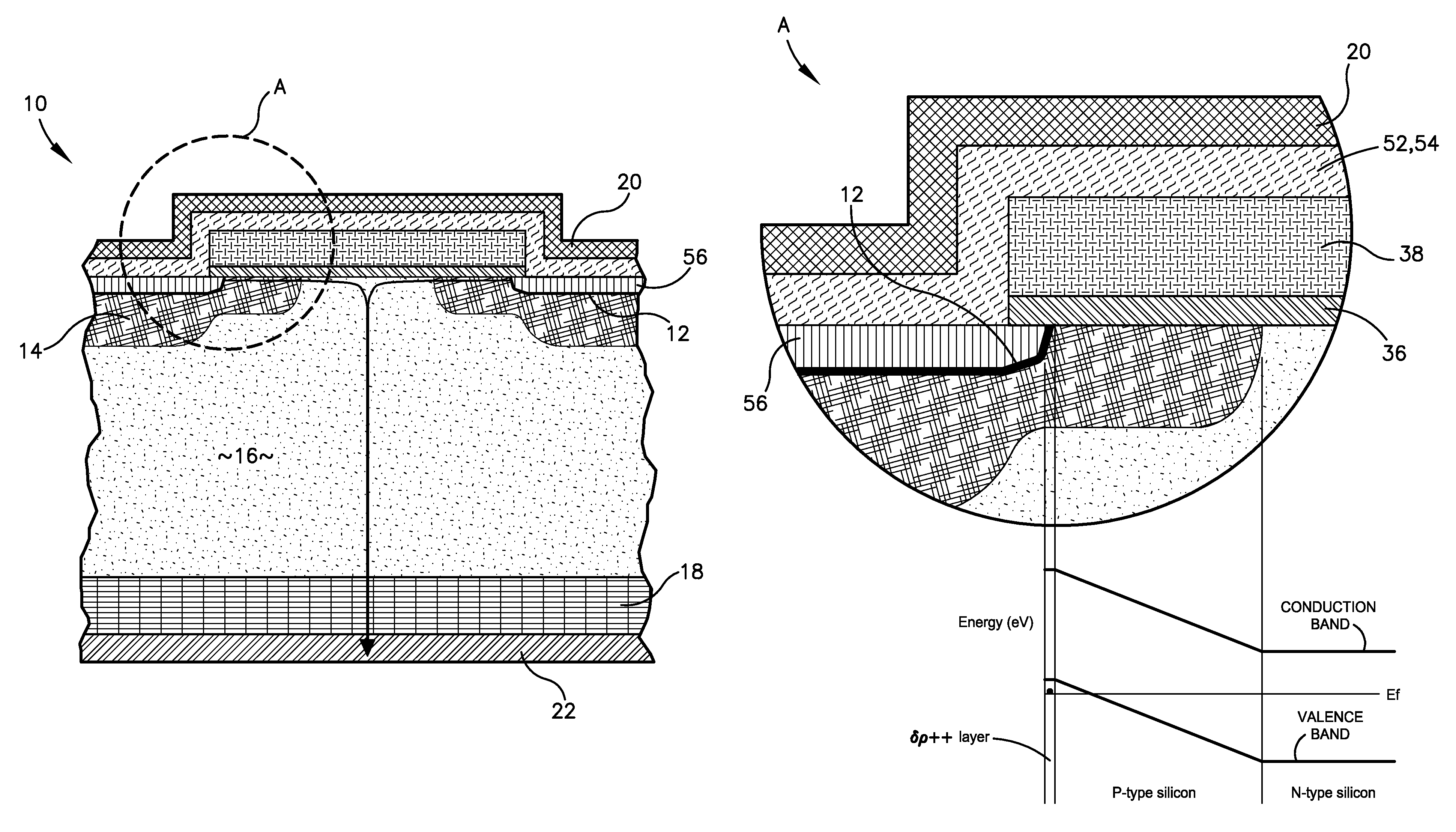
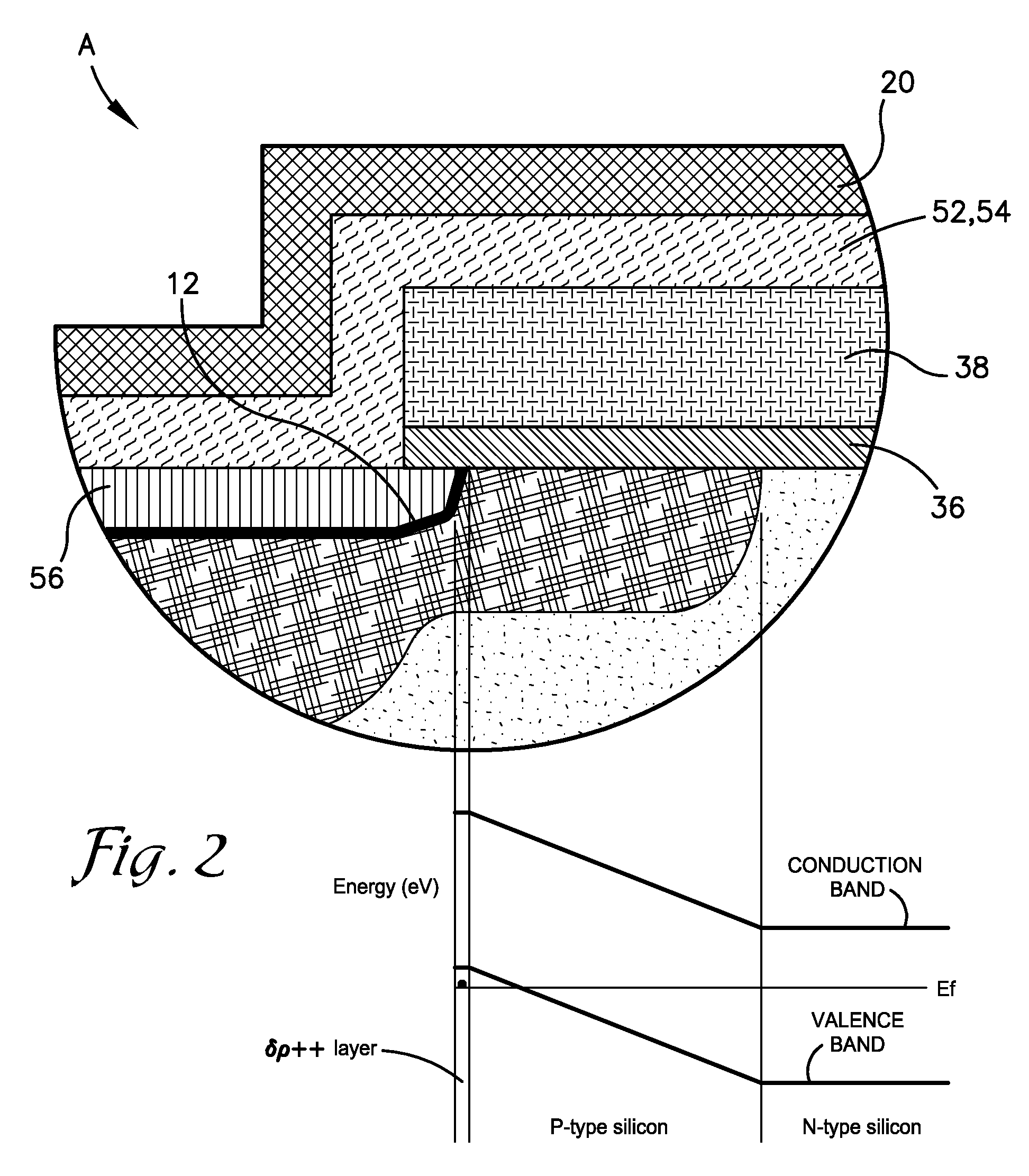
PatentActiveUS7847315B2
Innovation
- A semiconductor rectifier device comprising a supersaturated δP++ layer, a P-body region, an N-drift region, and an N+ substrate, with a method of fabrication involving dopant implantation and formation of titanium silicide to create a high-efficiency power semiconductor rectifier that operates as a pin diode or majority carrier device, reducing parasitic structures and improving switching performance.

Thermal Management Strategies for High-Power Applications
Thermal management represents one of the most critical challenges in high-power Schottky diode applications, where efficient heat dissipation directly impacts device performance, reliability, and operational lifespan. As power densities continue to increase in modern electronic systems, the ability to effectively manage thermal loads has become a determining factor in achieving superior rectification performance.
The fundamental challenge stems from the inherent characteristics of Schottky diodes in high-power scenarios. While these devices offer excellent switching speeds and low forward voltage drops, they generate significant heat during operation, particularly under high current conditions. The junction temperature must be maintained within acceptable limits to prevent thermal runaway, performance degradation, and premature device failure.
Advanced thermal interface materials have emerged as a cornerstone technology for high-power Schottky applications. Modern thermal interface materials, including phase-change materials and liquid metal compounds, can achieve thermal conductivities exceeding 15 W/mK, significantly improving heat transfer from the semiconductor junction to the heat sink. These materials fill microscopic air gaps and surface irregularities, creating more efficient thermal pathways.
Heat sink design optimization plays a crucial role in thermal management strategies. Advanced computational fluid dynamics modeling enables engineers to design heat sinks with optimized fin geometries, surface textures, and airflow patterns. Pin-fin and micro-channel heat sinks have demonstrated superior performance in high-power applications, with some designs achieving thermal resistances below 0.1°C/W for compact form factors.
Active cooling solutions are increasingly necessary for ultra-high-power applications. Liquid cooling systems, thermoelectric coolers, and vapor chamber technologies provide enhanced thermal management capabilities beyond conventional air cooling. These systems can maintain junction temperatures within optimal ranges even under extreme power conditions, enabling higher current densities and improved rectification efficiency.
Thermal monitoring and control systems integrate temperature sensors and feedback mechanisms to dynamically adjust operating parameters based on real-time thermal conditions. Smart thermal management algorithms can optimize performance while preventing thermal stress, extending device lifetime and maintaining consistent rectification characteristics across varying operational conditions.
Wide Bandgap Materials Integration in Schottky Devices
Wide bandgap (WBG) materials have emerged as transformative components in Schottky diode technology, fundamentally altering the performance landscape of rectification circuits. Silicon carbide (SiC) and gallium nitride (GaN) represent the most commercially viable WBG semiconductors, offering bandgap energies exceeding 3.0 eV compared to silicon's 1.12 eV. This substantial increase enables operation at higher temperatures, voltages, and frequencies while maintaining superior electrical characteristics.
The integration of SiC in Schottky devices has demonstrated remarkable improvements in breakdown voltage capabilities, with 4H-SiC substrates achieving electric field strengths exceeding 2.2 MV/cm. This enhanced field strength translates directly to reduced on-resistance and improved power density in rectification applications. GaN-based Schottky diodes exhibit exceptional switching characteristics, with reverse recovery times approaching zero due to their majority carrier conduction mechanism.
Manufacturing challenges in WBG integration primarily stem from substrate quality and epitaxial layer uniformity. SiC wafer production requires precise control of polytype formation, as crystal defects significantly impact device reliability. Advanced growth techniques including chemical vapor deposition and molecular beam epitaxy have enabled defect densities below 1 cm⁻² in commercial substrates.
Thermal management considerations become critical when implementing WBG materials, as their superior thermal conductivity must be properly utilized through optimized packaging solutions. SiC's thermal conductivity of 4.9 W/cm·K, compared to silicon's 1.5 W/cm·K, enables more compact designs with enhanced power handling capabilities.
Interface engineering between metal contacts and WBG semiconductors requires careful optimization of work function matching and barrier height control. Titanium, nickel, and platinum-based metallization schemes have shown promising results in achieving low-resistance ohmic contacts while maintaining thermal stability at elevated operating temperatures.
The economic viability of WBG integration continues improving as substrate costs decrease and manufacturing yields increase, making these materials increasingly attractive for high-performance rectification applications across automotive, aerospace, and renewable energy sectors.
Unlock deeper insights with PatSnap Eureka Quick Research — get a full tech report to explore trends and direct your research. Try now!
Generate Your Research Report Instantly with AI Agent
Supercharge your innovation with PatSnap Eureka AI Agent Platform!