Analysis of Transparent Transistor Production and Scalability
OCT 21, 202510 MIN READ
Generate Your Research Report Instantly with AI Agent
Patsnap Eureka helps you evaluate technical feasibility & market potential.
Transparent Transistor Technology Evolution and Objectives
Transparent transistors have evolved significantly since their inception in the early 2000s, marking a revolutionary advancement in display and electronic technologies. Initially developed using amorphous oxide semiconductors, particularly indium gallium zinc oxide (IGZO), these transistors offered unprecedented combinations of optical transparency and electrical performance. The evolution trajectory began with rudimentary thin-film transistors exhibiting limited transparency and performance, progressing to today's highly efficient devices capable of supporting advanced display technologies and flexible electronics.
The fundamental technological breakthrough enabling transparent transistors was the development of transparent conducting oxides (TCOs) that could function as semiconducting materials while maintaining optical transparency. This innovation addressed the inherent contradiction between electrical conductivity and optical transparency that had previously limited electronic display technologies. Early iterations faced challenges with carrier mobility, stability, and manufacturing consistency, but systematic research efforts have progressively overcome these limitations.
Market demands have been a significant driver in transparent transistor evolution, with the display industry's push for higher resolution, lower power consumption, and form factor flexibility accelerating development. The emergence of OLED displays, wearable technologies, and augmented reality applications has further intensified research focus on transparent electronics that can deliver enhanced performance while maintaining invisibility in optical applications.
Current technological objectives center on several key parameters: improving carrier mobility to exceed 50 cm²/Vs while maintaining transparency above 80% in the visible spectrum; enhancing operational stability under various environmental conditions; reducing production costs through simplified manufacturing processes; and developing scalable production techniques compatible with large-area fabrication. Additionally, research aims to expand material options beyond traditional metal oxides to include organic semiconductors and 2D materials like graphene derivatives.
The roadmap for transparent transistor technology includes achieving fully flexible, stretchable transparent circuits capable of integration into next-generation wearable devices and smart surfaces. Long-term objectives include developing self-powered transparent electronics through integration with transparent energy harvesting systems, enabling autonomous operation in ambient environments. These advancements would support emerging applications in smart windows, transparent displays embedded in everyday surfaces, and invisible sensing networks for Internet of Things implementations.
Achieving these objectives requires interdisciplinary collaboration across materials science, electrical engineering, and manufacturing technology domains, with particular emphasis on nanoscale fabrication techniques and novel material synthesis methods that can maintain performance while enabling large-scale production.
Market Applications and Demand Analysis for Transparent Electronics
The transparent electronics market is experiencing robust growth driven by increasing demand for innovative display technologies and smart devices. Current market analysis indicates that transparent electronics, particularly transparent transistors, are becoming integral components in multiple high-growth sectors. The global transparent electronics market is projected to reach approximately 8.5 billion USD by 2026, with a compound annual growth rate exceeding 20% during the forecast period.
Consumer electronics represents the largest application segment, with transparent displays for smartphones, tablets, and wearable devices driving significant demand. The automotive industry follows closely, incorporating transparent displays in windshields and windows for augmented reality navigation systems and heads-up displays. This sector is expected to grow at over 25% annually as vehicle manufacturers increasingly adopt advanced driver assistance systems.
Smart buildings and architectural applications constitute another rapidly expanding market segment. Transparent solar cells integrated into windows and building facades are gaining traction as energy-efficient solutions. This segment is projected to grow substantially as green building initiatives and energy conservation regulations become more stringent globally.
Healthcare applications present promising opportunities for transparent electronics, particularly in medical imaging displays and wearable health monitoring devices. The precision and clarity offered by transparent displays enhance diagnostic capabilities and patient monitoring efficiency. Market penetration in this sector is expected to accelerate as healthcare facilities upgrade their technological infrastructure.
Regional analysis reveals Asia-Pacific as the dominant market for transparent electronics manufacturing and consumption, with Japan, South Korea, and Taiwan leading in production capabilities. North America and Europe follow with strong research initiatives and premium application markets, particularly in automotive and healthcare sectors.
Consumer demand patterns indicate a growing preference for devices with enhanced visual interfaces and reduced form factors. Transparent displays address these preferences by offering improved aesthetics while maintaining or enhancing functionality. Market surveys show that consumers are willing to pay premium prices for devices incorporating transparent display technologies, particularly in high-end smartphones and wearables.
Industry forecasts suggest that as production scalability improves and manufacturing costs decrease, transparent electronics will penetrate mid-range consumer products, significantly expanding the addressable market. The development of flexible transparent electronics is expected to create entirely new application categories, potentially disrupting traditional device form factors across multiple industries.
Global Transparent Transistor Development Status and Barriers
Transparent transistor technology has evolved significantly over the past two decades, with major advancements occurring in materials science, fabrication techniques, and device architecture. Currently, the global development status shows varying levels of maturity across different regions, with East Asia, North America, and Europe leading research and commercialization efforts.
In East Asia, particularly Japan, South Korea, and Taiwan, transparent transistor development has reached advanced stages with several commercial applications already in the market. These regions benefit from strong display manufacturing ecosystems and substantial government investment in semiconductor research. Companies like Samsung, LG Display, and Sharp have established pilot production lines for transparent oxide semiconductor-based transistors.
North American development is characterized by strong fundamental research at universities and corporate R&D centers, with companies like Apple and Google investing in transparent electronics for next-generation display technologies. The focus remains primarily on novel materials and innovative device architectures rather than mass production capabilities.
European efforts are concentrated around research clusters in Germany, France, and the UK, with emphasis on sustainable manufacturing processes and specialized applications in automotive and medical sectors. The European Commission has funded several large-scale initiatives to strengthen the region's position in advanced electronic materials.
Despite these advancements, significant barriers impede widespread adoption and scalability of transparent transistor technology. The foremost challenge is manufacturing consistency at scale. While laboratory demonstrations show excellent performance, transferring these results to high-volume production environments introduces variability issues in transparency, conductivity, and stability parameters.
Material limitations present another substantial barrier. Current transparent conducting oxides like indium tin oxide (ITO) and indium gallium zinc oxide (IGZO) rely on indium, which faces supply constraints and price volatility. Alternative materials often compromise either transparency or electrical performance.
Process integration challenges also persist, particularly in achieving compatibility with existing display manufacturing infrastructure. The temperature sensitivity of many transparent semiconductor materials limits processing options and increases production complexity.
Stability and reliability under real-world conditions remain problematic, with performance degradation occurring due to environmental factors such as humidity, temperature fluctuations, and prolonged light exposure. This is particularly critical for applications requiring extended operational lifetimes.
Finally, cost considerations present a significant barrier to mass adoption. Current production methods for high-performance transparent transistors involve expensive deposition techniques and specialized equipment, resulting in higher manufacturing costs compared to conventional silicon-based technologies.
Current Manufacturing Approaches for Transparent Transistors
01 Metal oxide semiconductor materials for transparent transistors
Metal oxide semiconductors, such as zinc oxide, indium oxide, and indium-gallium-zinc oxide (IGZO), are widely used in the production of transparent transistors due to their high optical transparency and electrical conductivity. These materials can be deposited using various techniques including sputtering, atomic layer deposition, and solution processing methods, enabling the fabrication of high-performance transparent thin-film transistors (TFTs) for display applications.- Metal oxide semiconductor materials for transparent transistors: Metal oxide semiconductors, such as zinc oxide (ZnO), indium gallium zinc oxide (IGZO), and tin oxide, are widely used in the production of transparent transistors due to their high optical transparency and electrical conductivity. These materials can be deposited using various techniques including sputtering, atomic layer deposition, and solution processing methods, allowing for scalable manufacturing processes. The unique properties of these materials enable the fabrication of transistors that combine transparency with good electrical performance for display and electronic applications.
- Fabrication techniques for large-scale production: Various fabrication techniques have been developed to enable large-scale production of transparent transistors. These include roll-to-roll processing, inkjet printing, and photolithography adapted for transparent materials. These methods focus on achieving uniform deposition of semiconductor layers, precise patterning, and consistent electrical characteristics across large substrate areas. Innovations in these fabrication techniques have addressed challenges related to material compatibility, process temperature, and yield management, making commercial-scale production of transparent transistors increasingly viable.
- Integration with display technologies: Transparent transistors can be integrated with various display technologies, including LCD, OLED, and emerging flexible displays. The integration process involves specialized circuit design, addressing schemes, and interface protocols to ensure proper functioning of the display system. Transparent transistor arrays serve as the backplane for these displays, controlling individual pixels while maintaining optical clarity. This integration enables the development of transparent or semi-transparent display devices with applications in augmented reality, automotive heads-up displays, and smart windows.
- Performance optimization and stability enhancement: Enhancing the performance and stability of transparent transistors involves optimizing channel materials, gate dielectrics, and contact interfaces. Techniques such as surface passivation, doping control, and annealing processes are employed to improve carrier mobility, reduce threshold voltage shifts, and enhance long-term stability. Additionally, encapsulation methods protect the devices from environmental factors like moisture and oxygen, which can degrade performance over time. These optimization strategies are crucial for ensuring reliable operation in commercial applications.
- System architecture and computational modeling: System architecture design and computational modeling play crucial roles in scaling transparent transistor technology. Advanced simulation tools enable the prediction of electrical and optical properties, helping to optimize device structures before physical fabrication. Circuit design methodologies adapted for transparent electronics address unique challenges related to parasitic effects and signal integrity. Additionally, hierarchical system architectures facilitate the integration of transparent transistor arrays with conventional electronics, enabling complex functionality while maintaining scalability.
02 Scalable fabrication processes for transparent transistors
Scalable manufacturing processes for transparent transistors include roll-to-roll processing, large-area deposition techniques, and low-temperature fabrication methods. These approaches enable cost-effective production of transparent transistors on flexible substrates and large glass panels. Optimization of process parameters and equipment design is crucial for maintaining uniform electrical characteristics across large areas while ensuring high throughput and yield.Expand Specific Solutions03 Integration of transparent transistors in display technologies
Transparent transistors are integrated into various display technologies, including OLED, LCD, and emerging flexible displays. The integration process involves designing pixel circuits, addressing schemes, and interconnect structures that leverage the transparency of the transistors. This enables the creation of transparent or semi-transparent displays with improved aperture ratios, higher brightness, and lower power consumption compared to conventional opaque transistor-based displays.Expand Specific Solutions04 Performance optimization and stability enhancement
Enhancing the performance and stability of transparent transistors involves interface engineering, passivation techniques, and doping strategies. These approaches address challenges such as threshold voltage shifts, bias stress instability, and environmental degradation. Advanced materials and device architectures are developed to improve carrier mobility, on/off ratio, and operational stability under various environmental conditions, ensuring reliable operation in commercial applications.Expand Specific Solutions05 System architecture and computational methods for transparent electronics
System architectures and computational methods specifically designed for transparent electronics focus on optimizing data processing, memory management, and power distribution in transparent integrated circuits. These approaches include specialized algorithms, circuit designs, and system-on-chip configurations that accommodate the unique characteristics and constraints of transparent transistors, enabling efficient operation of transparent computing systems and display drivers.Expand Specific Solutions
Leading Companies and Research Institutions in Transparent Electronics
The transparent transistor market is currently in a growth phase, characterized by increasing demand for applications in displays, sensors, and flexible electronics. The market size is expanding rapidly, projected to reach significant value due to rising adoption in consumer electronics and automotive sectors. Technologically, the field shows varying maturity levels across different approaches. Academic institutions like Oregon State University, MIT, and Northwestern University are pioneering fundamental research, while commercial players demonstrate different specialization levels. Companies like Samsung Display, BOE Technology, and LG Display lead in display applications, while Semiconductor Energy Laboratory and TSMC focus on advanced manufacturing processes. Electronics & Telecommunications Research Institute and Industrial Technology Research Institute are bridging research-to-commercialization gaps, with emerging players like PragmatIC Semiconductor developing novel flexible electronics solutions.
Semiconductor Energy Laboratory Co., Ltd.
Technical Solution: Semiconductor Energy Laboratory (SEL) has pioneered oxide semiconductor technology for transparent transistors, particularly focusing on IGZO (Indium Gallium Zinc Oxide) materials. Their approach involves developing c-axis aligned crystalline IGZO (CAAC-IGZO) transistors that offer superior stability and performance compared to conventional amorphous IGZO. SEL's production methodology incorporates specialized sputtering techniques with precise oxygen partial pressure control during deposition, enabling the formation of highly ordered crystalline structures while maintaining transparency[1]. Their scalable manufacturing process integrates with existing TFT production lines, utilizing modified CVD and PVD systems that can deposit uniform IGZO films on large glass substrates up to Gen 10.5 (2940×3370mm)[2]. SEL has also developed proprietary annealing processes that reduce defect states at the semiconductor-insulator interface, significantly improving carrier mobility while preserving transparency above 80% in the visible spectrum[3].
Strengths: Industry-leading expertise in crystalline IGZO technology with superior stability against environmental stressors; established manufacturing infrastructure compatible with existing display production lines; extensive patent portfolio protecting their transparent transistor technologies. Weaknesses: Higher production costs compared to amorphous silicon; requires specialized deposition equipment; some performance limitations in extremely high-frequency applications.
BOE Technology Group Co., Ltd.
Technical Solution: BOE Technology has developed comprehensive transparent transistor production technology centered around oxide semiconductor materials, particularly focusing on indium-gallium-zinc-oxide (IGZO) and zinc-tin-oxide (ZTO) variants. Their manufacturing approach employs advanced sputtering systems with multi-zone temperature control, enabling precise deposition of oxide semiconductor layers with uniform thickness and composition across Gen 10.5 (2940×3370mm) substrates[1]. BOE's production methodology incorporates specialized annealing processes in controlled atmospheres that optimize the semiconductor's electrical properties while maintaining optical transparency. Their technology includes proprietary passivation layers that protect oxide semiconductors from environmental degradation and moisture ingress, significantly improving long-term stability[2]. BOE has also developed high-throughput photolithography processes specifically optimized for transparent transistor patterning, achieving feature sizes below 3μm across large substrate areas. Their manufacturing facilities implement automated optical inspection and electrical testing systems that can detect both visual and electrical defects in transparent transistor arrays, ensuring high yield rates in mass production[3]. BOE's transparent transistor technology achieves optical transparency exceeding 85% in the visible spectrum while maintaining electron mobility above 12 cm²/Vs.
Strengths: Industry-leading large-area substrate handling capabilities; extensive experience in display manufacturing; strong vertical integration from materials to finished products; competitive production costs through economies of scale. Weaknesses: Some limitations in achieving ultra-high frequency performance; challenges in maintaining uniform electrical characteristics across extremely large substrates; relatively higher defect rates compared to smaller substrate technologies.
Key Patents and Scientific Breakthroughs in Transparent Semiconductors
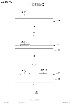
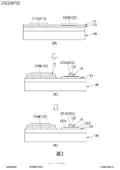
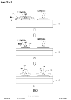
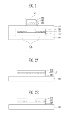
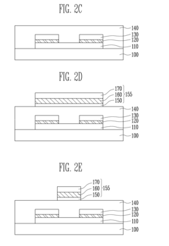
Manufacturing method of transparent thin film transistor with simplified process capable of sputtering the patterned dielectric layer, the patterned channel layer and the passivation layer without additional ion implantation processes
PatentActiveTW202238732A
Innovation
- A simplified manufacturing method for transparent TFTs using sputtering techniques to form a patterned gate dielectric layer, channel layer, and passivation layer without flammable gases, eliminating the need for ion implantation and reducing the number of photomasks.

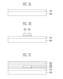
Method of manufacturing transparent transistor with multi-layered structures
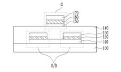
PatentInactiveUS20130189816A1
Innovation
- A stacked structure for transparent transistors is developed, comprising a substrate with source and drain electrodes having a multi-layered structure of a lower transparent layer, a metal layer, and an upper transparent layer, where the lower and upper transparent layers are formed of the same semiconductor material, and a gate electrode is aligned with the channel, allowing for improved transparency and conductivity through the use of nitride layers with a refractive index of 2.0 or higher.
Scalability Challenges and Mass Production Feasibility
The scaling of transparent transistor technology from laboratory prototypes to mass production presents significant challenges that must be addressed for commercial viability. Current manufacturing processes for transparent transistors often rely on specialized equipment and precise environmental controls that are difficult to replicate at industrial scales. The primary obstacle lies in maintaining consistent material properties across large substrate areas while ensuring high yield rates and acceptable performance metrics.
Temperature sensitivity during deposition processes represents a critical challenge, as even minor variations can lead to inconsistent film formation and compromised electrical properties. This is particularly problematic for oxide-based transparent semiconductors such as IGZO (Indium Gallium Zinc Oxide), where oxygen vacancy concentration—a key determinant of carrier mobility—is highly dependent on processing conditions.
Equipment compatibility presents another significant hurdle. Many transparent transistor fabrication techniques developed in research settings utilize custom-built or modified equipment that lacks standardization for high-volume manufacturing environments. The transition to industry-standard tools often requires substantial process re-engineering and optimization, extending development timelines and increasing costs.
Cost considerations further complicate scalability efforts. The reliance on rare elements like indium in many transparent conductor formulations introduces supply chain vulnerabilities and price volatility risks. While alternative materials are being explored, they frequently exhibit performance trade-offs that may limit application potential.
Defect density management becomes increasingly challenging at larger scales. Particulate contamination, surface roughness variations, and interface quality issues that might be manageable in small-scale production can become yield-limiting factors in mass manufacturing scenarios. Advanced in-line metrology and process control systems are essential but add complexity to production lines.
Integration with existing manufacturing infrastructure represents a practical consideration often overlooked in academic research. The ideal transparent transistor technology should be compatible with established production lines to minimize capital investment requirements. Technologies requiring entirely new fabrication paradigms face significant barriers to adoption regardless of performance advantages.
Recent advances in roll-to-roll processing and solution-based deposition methods show promise for overcoming some scalability limitations, potentially enabling high-throughput production of flexible transparent electronics. However, these approaches still require substantial development to match the performance consistency achieved through conventional vacuum-based techniques.
Environmental Impact and Sustainability of Transparent Electronics Manufacturing
The manufacturing processes for transparent transistors present significant environmental challenges that must be addressed for sustainable industry growth. Traditional semiconductor fabrication techniques involve energy-intensive processes and hazardous materials that pose environmental risks. Transparent electronics manufacturing specifically utilizes rare materials like indium tin oxide (ITO) and zinc oxide, which face resource scarcity concerns and environmentally problematic extraction methods.
Energy consumption represents a major sustainability challenge in transparent transistor production. The high-temperature processes required for material deposition and annealing consume substantial electricity, contributing to carbon emissions when powered by non-renewable sources. Industry data indicates that fabrication facilities for transparent electronics can consume between 30-50 million kWh annually, comparable to powering 3,000-5,000 households.
Water usage presents another critical environmental concern. Semiconductor manufacturing typically requires ultra-pure water for cleaning and processing, with estimates suggesting 5-10 million gallons of water consumption per day in large fabrication facilities. Transparent electronics manufacturing, while generally less water-intensive than traditional silicon processing, still requires significant water resources that must be managed sustainably.
Chemical waste management remains particularly challenging. The etching processes used in transparent transistor fabrication generate acidic and metallic waste streams that require specialized treatment. Additionally, certain precursor materials used in metal oxide deposition contain volatile organic compounds (VOCs) that contribute to air pollution if not properly controlled.
Recent sustainability initiatives have focused on developing eco-friendly alternatives to traditional manufacturing approaches. Low-temperature solution processing methods have emerged as promising techniques that reduce energy consumption by 40-60% compared to vacuum-based deposition. These approaches also enable the use of biodegradable substrates, potentially creating pathways toward fully recyclable transparent electronic devices.
Material innovation represents another avenue toward sustainability. Research into earth-abundant alternatives to indium-based transparent conductors has accelerated, with aluminum-doped zinc oxide (AZO) and fluorine-doped tin oxide (FTO) showing promise as more sustainable options. Additionally, closed-loop recycling systems for recovering rare materials from manufacturing waste and end-of-life products are being developed, with recovery rates reaching 60-80% efficiency in pilot programs.
Regulatory frameworks are increasingly influencing manufacturing practices, with the European Union's Restriction of Hazardous Substances (RoHS) directive and similar regulations worldwide driving the transition toward greener production methods. Companies investing in sustainable manufacturing not only reduce environmental impact but also gain competitive advantages through reduced resource costs and improved brand reputation.
Unlock deeper insights with Patsnap Eureka Quick Research — get a full tech report to explore trends and direct your research. Try now!
Generate Your Research Report Instantly with AI Agent
Supercharge your innovation with Patsnap Eureka AI Agent Platform!