
Capacitance Modulation in Ferroelectric Tunnel Junctions
OCT 13, 20259 MIN READ
Generate Your Research Report Instantly with AI Agent
Patsnap Eureka helps you evaluate technical feasibility & market potential.
Ferroelectric Tunnel Junction Background and Objectives
Ferroelectric Tunnel Junctions (FTJs) represent a significant advancement in the field of non-volatile memory technologies, emerging from decades of research in ferroelectric materials and quantum tunneling phenomena. The concept of FTJs was theoretically proposed in the early 1970s, but practical implementations only became feasible in the early 2000s with advancements in thin-film deposition techniques that enabled the creation of ultrathin ferroelectric barriers.
The evolution of FTJs has been closely tied to the broader development of ferroelectric materials, which began with the discovery of ferroelectricity in Rochelle salt in 1920 and progressed through the identification of various perovskite-structured ferroelectrics such as BaTiO3, PbTiO3, and PZT in the mid-20th century. More recently, HfO2-based ferroelectrics have gained prominence due to their CMOS compatibility and scalability advantages.
Capacitance modulation in FTJs represents a particularly intriguing aspect of these devices, as it offers a mechanism to electrically control the tunneling barrier properties through polarization switching. This phenomenon arises from the interplay between ferroelectric polarization and the screening charges at the electrode interfaces, resulting in modulation of the effective barrier height and width.
The technical objectives in this field are multifaceted and ambitious. Primary goals include achieving reliable and reproducible capacitance modulation with high ON/OFF ratios, extending device endurance beyond 10^10 cycles, and reducing operating voltages to sub-1V levels for compatibility with modern integrated circuits. Additionally, there is significant interest in understanding and exploiting the fundamental physics of capacitance modulation to develop novel functionalities.
Another critical objective is the integration of FTJs with conventional semiconductor technologies, particularly CMOS, which requires addressing challenges related to materials compatibility, process integration, and scalability. The development of FTJs with dimensions below 10 nm while maintaining robust ferroelectric properties represents a significant technical hurdle that must be overcome.
From a broader perspective, researchers aim to leverage capacitance modulation in FTJs to enable new computing paradigms, including neuromorphic computing architectures that mimic the brain's functionality. The analog nature of polarization switching in ferroelectric materials offers promising opportunities for implementing synaptic weight functions in artificial neural networks.
The convergence of these technical objectives with recent advances in materials science and nanofabrication techniques has positioned FTJs as a promising technology for next-generation memory and computing applications, driving continued research and development efforts in this dynamic field.
The evolution of FTJs has been closely tied to the broader development of ferroelectric materials, which began with the discovery of ferroelectricity in Rochelle salt in 1920 and progressed through the identification of various perovskite-structured ferroelectrics such as BaTiO3, PbTiO3, and PZT in the mid-20th century. More recently, HfO2-based ferroelectrics have gained prominence due to their CMOS compatibility and scalability advantages.
Capacitance modulation in FTJs represents a particularly intriguing aspect of these devices, as it offers a mechanism to electrically control the tunneling barrier properties through polarization switching. This phenomenon arises from the interplay between ferroelectric polarization and the screening charges at the electrode interfaces, resulting in modulation of the effective barrier height and width.
The technical objectives in this field are multifaceted and ambitious. Primary goals include achieving reliable and reproducible capacitance modulation with high ON/OFF ratios, extending device endurance beyond 10^10 cycles, and reducing operating voltages to sub-1V levels for compatibility with modern integrated circuits. Additionally, there is significant interest in understanding and exploiting the fundamental physics of capacitance modulation to develop novel functionalities.
Another critical objective is the integration of FTJs with conventional semiconductor technologies, particularly CMOS, which requires addressing challenges related to materials compatibility, process integration, and scalability. The development of FTJs with dimensions below 10 nm while maintaining robust ferroelectric properties represents a significant technical hurdle that must be overcome.
From a broader perspective, researchers aim to leverage capacitance modulation in FTJs to enable new computing paradigms, including neuromorphic computing architectures that mimic the brain's functionality. The analog nature of polarization switching in ferroelectric materials offers promising opportunities for implementing synaptic weight functions in artificial neural networks.
The convergence of these technical objectives with recent advances in materials science and nanofabrication techniques has positioned FTJs as a promising technology for next-generation memory and computing applications, driving continued research and development efforts in this dynamic field.
Market Applications for Capacitance Modulation Technologies
Capacitance modulation in Ferroelectric Tunnel Junctions (FTJs) represents a transformative technology with diverse market applications across multiple industries. The ability to precisely control and modulate capacitance at the nanoscale offers significant advantages for next-generation electronic devices and systems.
In the semiconductor industry, FTJ-based capacitance modulation technologies are poised to revolutionize memory architectures. The market for non-volatile memory solutions continues to expand rapidly, with particular demand for low-power, high-density storage solutions. FTJ-based memory cells leverage capacitance modulation to store binary or multi-state information, potentially offering superior performance compared to conventional flash memory in terms of switching speed, endurance, and energy efficiency.
The neuromorphic computing sector represents another promising market application. As artificial intelligence and machine learning continue to advance, there is growing demand for hardware architectures that can efficiently implement neural network operations. FTJ-based synaptic devices utilizing capacitance modulation can mimic biological synapses, enabling more efficient implementation of neuromorphic systems. This market segment is expected to grow substantially as edge computing and AI applications proliferate across consumer electronics, automotive systems, and industrial automation.
Radio frequency (RF) and microwave engineering applications constitute another significant market opportunity. Tunable capacitors based on ferroelectric materials enable the development of reconfigurable RF components such as filters, phase shifters, and matching networks. These components are essential for advanced communication systems, including 5G infrastructure and future 6G technologies, where dynamic spectrum allocation and adaptive signal processing are critical requirements.
The sensor market represents yet another application domain for capacitance modulation technologies. FTJ-based sensors can detect minute changes in environmental conditions, mechanical stress, or chemical composition through variations in capacitance. This capability is particularly valuable for Internet of Things (IoT) applications, environmental monitoring, and biomedical devices where high sensitivity, low power consumption, and miniaturization are essential requirements.
Quantum computing, though still emerging, presents a long-term market opportunity for capacitance modulation technologies. FTJs could potentially serve as quantum bits (qubits) or auxiliary components in quantum computing architectures, leveraging their unique electrical properties and nanoscale dimensions.
The automotive industry is increasingly adopting advanced electronics for autonomous driving, safety systems, and infotainment. FTJ-based capacitance modulation technologies offer potential applications in high-reliability memory systems, sensor interfaces, and power management circuits designed to operate in harsh automotive environments.
In the semiconductor industry, FTJ-based capacitance modulation technologies are poised to revolutionize memory architectures. The market for non-volatile memory solutions continues to expand rapidly, with particular demand for low-power, high-density storage solutions. FTJ-based memory cells leverage capacitance modulation to store binary or multi-state information, potentially offering superior performance compared to conventional flash memory in terms of switching speed, endurance, and energy efficiency.
The neuromorphic computing sector represents another promising market application. As artificial intelligence and machine learning continue to advance, there is growing demand for hardware architectures that can efficiently implement neural network operations. FTJ-based synaptic devices utilizing capacitance modulation can mimic biological synapses, enabling more efficient implementation of neuromorphic systems. This market segment is expected to grow substantially as edge computing and AI applications proliferate across consumer electronics, automotive systems, and industrial automation.
Radio frequency (RF) and microwave engineering applications constitute another significant market opportunity. Tunable capacitors based on ferroelectric materials enable the development of reconfigurable RF components such as filters, phase shifters, and matching networks. These components are essential for advanced communication systems, including 5G infrastructure and future 6G technologies, where dynamic spectrum allocation and adaptive signal processing are critical requirements.
The sensor market represents yet another application domain for capacitance modulation technologies. FTJ-based sensors can detect minute changes in environmental conditions, mechanical stress, or chemical composition through variations in capacitance. This capability is particularly valuable for Internet of Things (IoT) applications, environmental monitoring, and biomedical devices where high sensitivity, low power consumption, and miniaturization are essential requirements.
Quantum computing, though still emerging, presents a long-term market opportunity for capacitance modulation technologies. FTJs could potentially serve as quantum bits (qubits) or auxiliary components in quantum computing architectures, leveraging their unique electrical properties and nanoscale dimensions.
The automotive industry is increasingly adopting advanced electronics for autonomous driving, safety systems, and infotainment. FTJ-based capacitance modulation technologies offer potential applications in high-reliability memory systems, sensor interfaces, and power management circuits designed to operate in harsh automotive environments.
Current Challenges in Ferroelectric Tunnel Junction Development
Despite significant advancements in ferroelectric tunnel junction (FTJ) technology, several critical challenges continue to impede their widespread implementation and commercialization. The primary obstacle remains the reliable control and modulation of capacitance in these devices, particularly when scaling down to nanometer dimensions. As device size decreases, quantum mechanical effects become increasingly dominant, leading to unpredictable tunneling behaviors that complicate precise capacitance modulation.
Material stability presents another significant challenge, with many ferroelectric materials exhibiting degradation in their polarization properties over time. This degradation, known as fatigue, substantially reduces the effective lifetime of FTJ devices and limits their practical applications in memory and logic circuits. Additionally, the interface quality between the ferroelectric layer and the electrodes critically affects tunneling efficiency, with atomic-level defects potentially causing significant performance variations.
Temperature sensitivity remains a persistent issue, as many ferroelectric materials lose their polarization properties at temperatures commonly encountered in electronic devices. This thermal instability restricts the operating temperature range of FTJs and necessitates additional cooling systems in practical applications, increasing system complexity and cost.
Manufacturing consistency poses a substantial hurdle for mass production. Current fabrication techniques struggle to produce uniform ferroelectric layers with consistent thickness and crystalline structure across large wafers, resulting in device-to-device performance variations that are unacceptable for commercial applications.
The integration of FTJs with conventional CMOS technology presents compatibility challenges, particularly regarding process temperatures and material interactions. Many ferroelectric materials require high-temperature processing that can damage surrounding CMOS components, necessitating the development of low-temperature deposition techniques without sacrificing ferroelectric quality.
Power consumption during switching operations remains higher than theoretical predictions, limiting the energy efficiency advantages that initially made FTJs attractive for low-power applications. The energy required to switch polarization states increases with cycling, further complicating power management in FTJ-based systems.
Finally, there exists a fundamental knowledge gap in understanding the complex interplay between ferroelectric domain dynamics and tunneling mechanisms. This theoretical limitation hinders the development of accurate models for predicting device behavior and optimizing design parameters. Advanced characterization techniques and computational models are needed to bridge this gap and enable more systematic approaches to FTJ development.
Material stability presents another significant challenge, with many ferroelectric materials exhibiting degradation in their polarization properties over time. This degradation, known as fatigue, substantially reduces the effective lifetime of FTJ devices and limits their practical applications in memory and logic circuits. Additionally, the interface quality between the ferroelectric layer and the electrodes critically affects tunneling efficiency, with atomic-level defects potentially causing significant performance variations.
Temperature sensitivity remains a persistent issue, as many ferroelectric materials lose their polarization properties at temperatures commonly encountered in electronic devices. This thermal instability restricts the operating temperature range of FTJs and necessitates additional cooling systems in practical applications, increasing system complexity and cost.
Manufacturing consistency poses a substantial hurdle for mass production. Current fabrication techniques struggle to produce uniform ferroelectric layers with consistent thickness and crystalline structure across large wafers, resulting in device-to-device performance variations that are unacceptable for commercial applications.
The integration of FTJs with conventional CMOS technology presents compatibility challenges, particularly regarding process temperatures and material interactions. Many ferroelectric materials require high-temperature processing that can damage surrounding CMOS components, necessitating the development of low-temperature deposition techniques without sacrificing ferroelectric quality.
Power consumption during switching operations remains higher than theoretical predictions, limiting the energy efficiency advantages that initially made FTJs attractive for low-power applications. The energy required to switch polarization states increases with cycling, further complicating power management in FTJ-based systems.
Finally, there exists a fundamental knowledge gap in understanding the complex interplay between ferroelectric domain dynamics and tunneling mechanisms. This theoretical limitation hinders the development of accurate models for predicting device behavior and optimizing design parameters. Advanced characterization techniques and computational models are needed to bridge this gap and enable more systematic approaches to FTJ development.
State-of-the-Art Capacitance Modulation Mechanisms
01 Structure and fabrication of ferroelectric tunnel junctions
Ferroelectric tunnel junctions (FTJs) consist of two electrodes separated by a thin ferroelectric barrier. The fabrication process involves depositing ferroelectric materials like BaTiO3 or PZT between conductive electrodes. The tunnel barrier thickness is critical, typically a few nanometers, to allow quantum tunneling while maintaining ferroelectric properties. Various deposition techniques such as pulsed laser deposition, sputtering, or atomic layer deposition can be used to create these structures with precise control of layer thickness and interfaces.- Structure and design of ferroelectric tunnel junctions: Ferroelectric tunnel junctions (FTJs) consist of two electrodes separated by a thin ferroelectric barrier. The structure typically includes a ferroelectric layer sandwiched between conductive materials, allowing for quantum tunneling effects. The design of these junctions can be optimized by controlling the thickness of the ferroelectric layer, selecting appropriate electrode materials, and engineering the interfaces between layers to enhance capacitance properties and tunneling efficiency.
- Capacitance modulation in ferroelectric tunnel junctions: The capacitance of ferroelectric tunnel junctions can be modulated by controlling the polarization state of the ferroelectric material. This modulation occurs due to changes in the charge distribution at the interfaces between the ferroelectric layer and the electrodes. The capacitance exhibits hysteretic behavior corresponding to the polarization switching of the ferroelectric material, allowing for multiple stable states that can be utilized in memory applications.
- Materials for enhanced capacitance in ferroelectric tunnel junctions: Various materials can be used to enhance the capacitance properties of ferroelectric tunnel junctions. Common ferroelectric materials include barium titanate (BaTiO3), lead zirconate titanate (PZT), and hafnium oxide-based compounds. The selection of electrode materials also plays a crucial role, with metals like platinum, titanium nitride, or conductive oxides being commonly used. Doping and compositional engineering of these materials can further optimize the capacitance characteristics and tunneling behavior.
- Measurement and characterization of capacitance in ferroelectric tunnel junctions: Specialized techniques are employed to measure and characterize the capacitance in ferroelectric tunnel junctions. These include impedance spectroscopy, capacitance-voltage (C-V) profiling, and scanning probe microscopy methods. The capacitance measurements often need to account for the ultrathin nature of the ferroelectric layer and the quantum mechanical effects that influence charge transport. These characterization methods help in understanding the relationship between ferroelectric polarization and capacitance behavior.
- Applications of capacitance effects in ferroelectric tunnel junctions: The capacitance properties of ferroelectric tunnel junctions enable various applications in electronic devices. These include non-volatile memory elements, neuromorphic computing components, and tunable capacitors for RF applications. The non-linear capacitance behavior can be exploited for multi-state storage, while the low power consumption and high switching speed make these junctions attractive for energy-efficient computing architectures. The capacitance effects also contribute to the development of novel sensors and energy harvesting devices.
02 Capacitance characteristics and measurement in FTJs
The capacitance of ferroelectric tunnel junctions exhibits unique characteristics due to the ferroelectric polarization switching. Capacitance-voltage (C-V) measurements show hysteresis behavior corresponding to the polarization states. The capacitance value depends on the ferroelectric layer thickness, area, and material properties. Advanced measurement techniques including impedance spectroscopy and scanning probe microscopy can be used to characterize the capacitance behavior at different frequencies and under various bias conditions, providing insights into the polarization dynamics and charge distribution at interfaces.Expand Specific Solutions03 Polarization effects on tunneling and capacitance
The polarization state of the ferroelectric layer significantly affects the tunneling current and capacitance in FTJs. When the polarization direction changes, the potential barrier height and width are modified, leading to changes in the tunneling probability and capacitance. This electrostatic effect creates a high resistance state and a low resistance state that can be used for memory applications. The capacitance shows distinct values corresponding to different polarization states, allowing for multi-state memory capabilities and analog computing functionalities.Expand Specific Solutions04 Integration of FTJs in memory and computing devices
Ferroelectric tunnel junctions can be integrated into various memory and computing architectures. Their non-volatile nature, low power consumption, and scalability make them promising candidates for next-generation memory devices. FTJs can be incorporated into crossbar arrays for high-density storage or integrated with CMOS technology for hybrid computing systems. The capacitance characteristics of FTJs enable analog computing applications such as neuromorphic computing, where the continuous range of capacitance values can represent synaptic weights in artificial neural networks.Expand Specific Solutions05 Material engineering for enhanced capacitance properties
Various material engineering approaches can enhance the capacitance properties of ferroelectric tunnel junctions. Doping the ferroelectric layer with specific elements can modify the polarization characteristics and improve retention. Interface engineering between the electrodes and ferroelectric layer can reduce depolarization fields and enhance capacitance stability. Multilayer structures combining different ferroelectric materials or incorporating dielectric layers can optimize the capacitance-voltage behavior. Additionally, strain engineering through lattice mismatch with the substrate can enhance the ferroelectric properties and resulting capacitance characteristics.Expand Specific Solutions
Leading Research Groups and Companies in FTJ Technology
Ferroelectric Tunnel Junctions (FTJs) with capacitance modulation capabilities are currently in an early growth phase, with the market expected to expand significantly as applications in neuromorphic computing and non-volatile memory emerge. The global market remains relatively small but is projected to grow as technical challenges are overcome. Research institutions like CNRS, Peking University, and Tsinghua University are driving fundamental advances, while industry players including IBM, Samsung, and TSMC are exploring commercial applications. Companies like Huawei and Thales are investing in FTJ technology for security and computing applications. The technology is approaching maturity for specific applications, with major semiconductor manufacturers (TSMC, Applied Materials) beginning to incorporate FTJs into their roadmaps, though challenges in scalability and integration persist.
Centre National de la Recherche Scientifique
Technical Solution: CNRS在铁电隧道结(FTJs)电容调制领域处于领先地位,开发了基于BaTiO3/La0.67Sr0.33MnO3异质结构的FTJ技术。其研究团队通过精确控制铁电层厚度(2-3nm)实现了显著的电阻调制比(ON/OFF比>100)。CNRS的技术方案特别关注铁电极化反转过程中的电容变化机制,通过引入中间氧化物层(如SrTiO3)作为缓冲层,有效改善了界面特性和电容调制效果。他们的实验证明,在室温下可实现稳定的电容调制,并通过脉冲宽度调制实现多值存储功能。CNRS还开发了专用测量技术,能够同时监测FTJ中的电阻和电容变化,为理解铁电隧道结中的物理机制提供了重要工具。
优势:拥有世界领先的铁电材料研究团队和先进表征设备,在铁电隧道结基础理论研究方面处于前沿;能够实现纳米尺度铁电薄膜的精确生长和表征。劣势:技术商业化进程相对缓慢,与产业界的合作网络有待加强;在大规模集成方面的经验不足。
International Business Machines Corp.
Technical Solution: IBM在铁电隧道结电容调制领域开发了独特的"混合铁电-自旋电子"技术方案。该方案结合了铁电材料(如HfZrO2)与磁性隧道结构,创造了多功能存储单元。IBM的技术利用铁电极化不仅调制电阻,还同时调制电容特性,实现了双重信息编码机制。其核心创新在于采用原子层沉积(ALD)技术精确控制铁电层厚度(1.5-3nm),并通过特殊的电极材料选择(如TiN/Hf0.5Zr0.5O2/SrRuO3结构)优化了界面特性。IBM还开发了专有的"渐变极化"技术,通过施加不同幅值的电压脉冲,实现了连续可调的电容值,使单个FTJ单元可存储多比特信息。该技术在300mm晶圆上已实现了初步集成,展示了与CMOS工艺的兼容性,并在低温(4.2K)和室温条件下均表现出稳定的电容调制特性。
优势:拥有强大的材料科学和器件工程能力,能够将实验室技术快速转化为可量产的解决方案;在CMOS兼容性和大规模集成方面具有丰富经验。劣势:在极低温环境下的铁电隧道结性能优化仍面临挑战;技术复杂度高,可能增加制造成本和难度。
Key Patents and Scientific Breakthroughs in FTJ Technology
Ferroelectric tunnel junctions with conductive electrodes having asymmetric nitrogen or oxygen profiles
PatentActiveUS12408349B2
Innovation
- The ferroelectric tunnel junctions are designed with electrodes containing varying percentages of nitrogen or oxygen, leading to different thicknesses of interfacial layers and work functions, enhancing tunneling current and device performance.


Ferroelectric tunnel FET switch and memory
PatentActiveUS8362604B2
Innovation
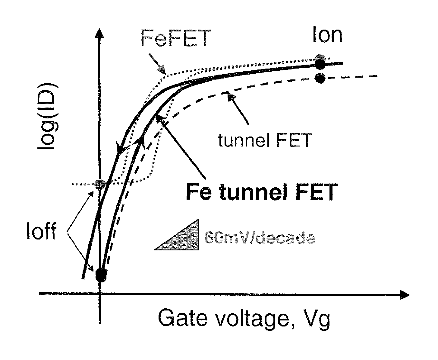
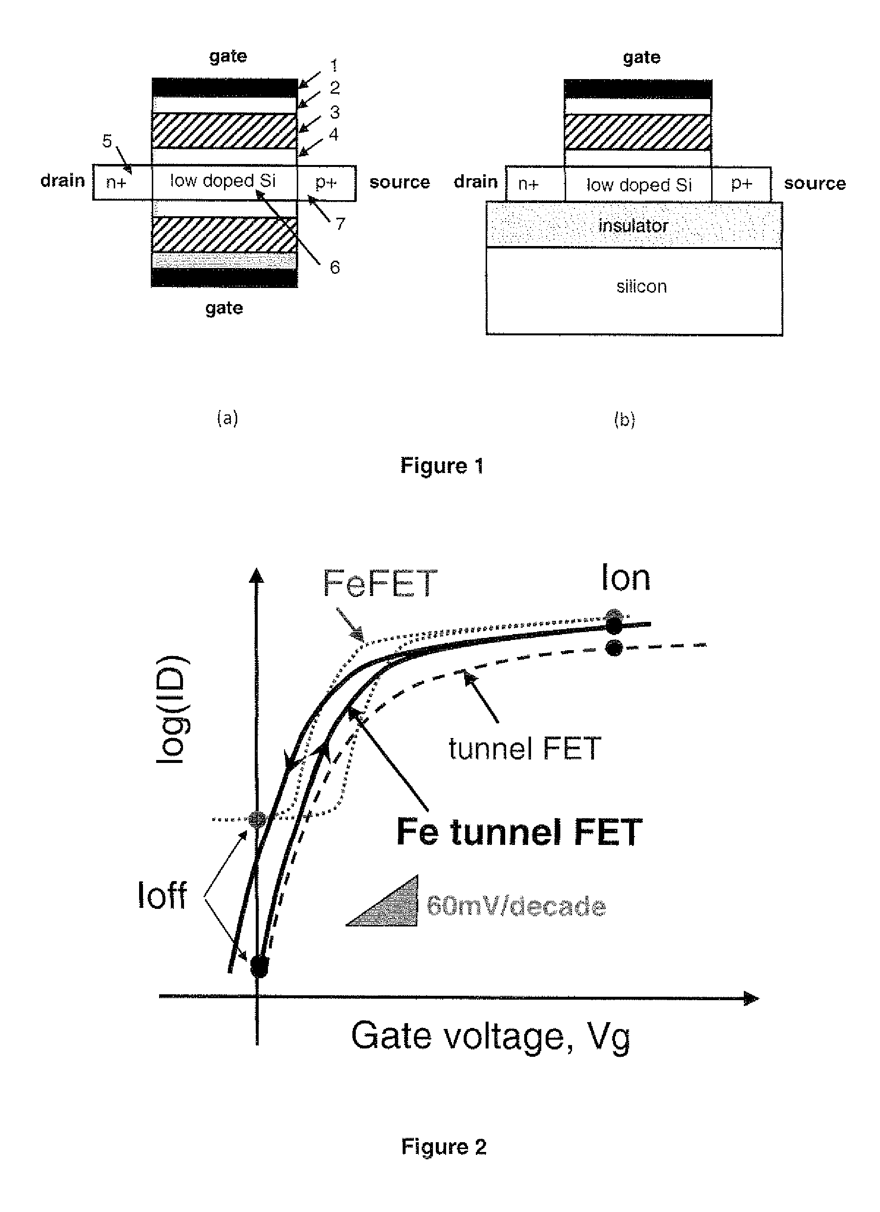
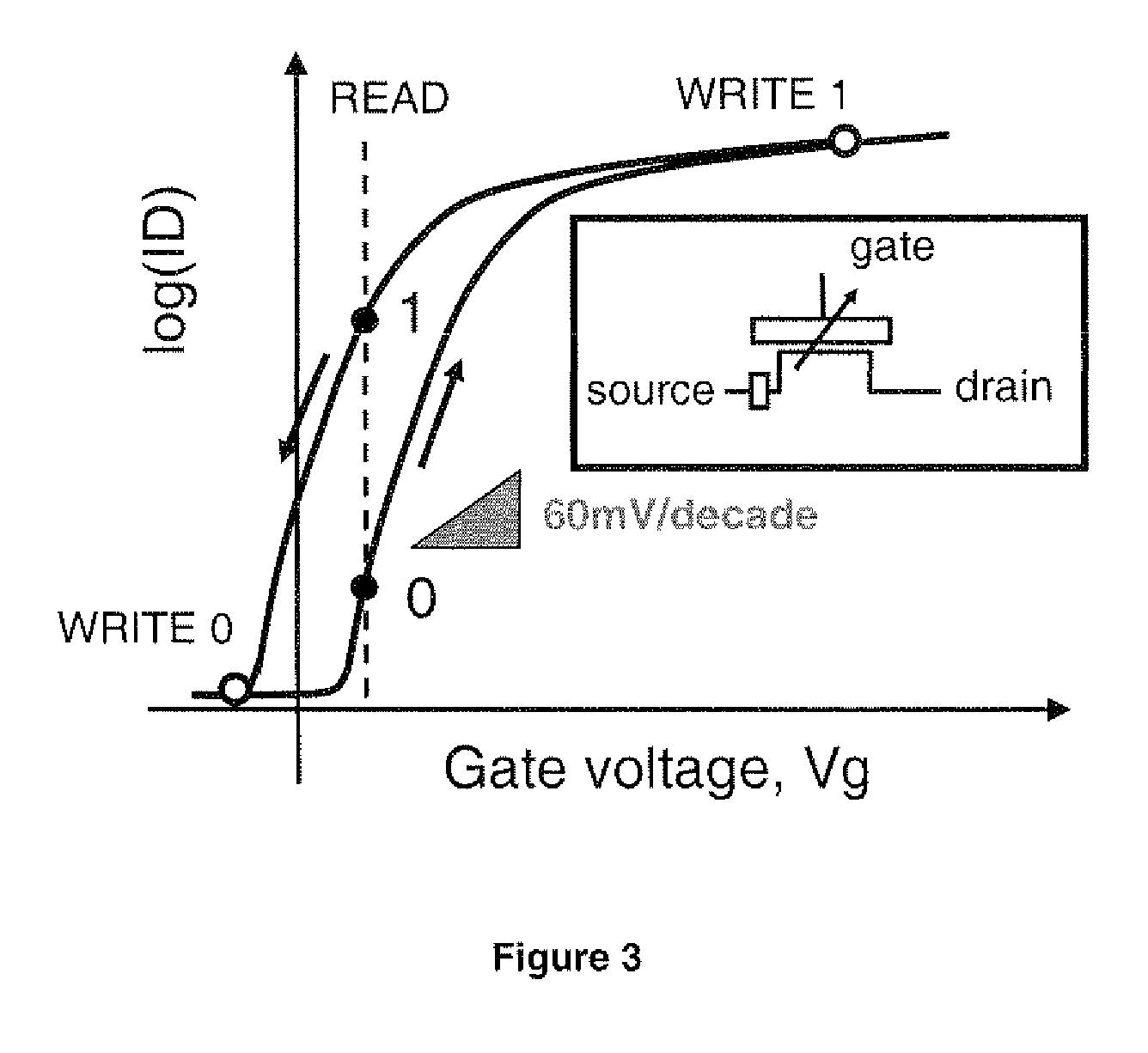
- A ferroelectric Tunnel FET combining band-to-band tunneling and negative capacitance principles in a single device architecture, utilizing a ferroelectric gate stack for steep transitions and low off-current, enabling lower voltage and power operation.

Materials Science Advancements for FTJ Performance
Recent advancements in materials science have significantly enhanced the performance of Ferroelectric Tunnel Junctions (FTJs), particularly in relation to capacitance modulation capabilities. The selection and engineering of ferroelectric materials represent the cornerstone of these developments, with hafnium oxide (HfO2) emerging as a particularly promising candidate due to its CMOS compatibility and robust ferroelectric properties at nanoscale dimensions.
The thickness optimization of ferroelectric layers has proven critical for maximizing the tunneling electroresistance (TER) ratio while maintaining sufficient capacitance modulation. Research indicates that ferroelectric layers between 2-5 nm provide optimal performance, balancing quantum tunneling requirements with ferroelectric stability. This precise dimensional control has been achieved through advanced deposition techniques such as atomic layer deposition (ALD) and pulsed laser deposition (PLD).
Interface engineering between ferroelectric materials and electrodes has emerged as another crucial factor in enhancing FTJ performance. The introduction of buffer layers and careful management of termination chemistry at these interfaces has demonstrated significant improvements in polarization stability and switching characteristics. Recent studies have shown that controlling oxygen vacancies at these interfaces can dramatically influence the capacitance modulation range.
Electrode material selection has evolved beyond simple conductivity considerations to include work function engineering and lattice matching properties. Platinum, titanium nitride, and strontium ruthenate have shown particular promise as electrode materials that maintain ferroelectric properties while facilitating efficient charge transfer across the junction.
Doping strategies have revolutionized the performance envelope of ferroelectric materials in FTJs. Strategic incorporation of elements such as aluminum, silicon, or zirconium into HfO2-based ferroelectrics has enhanced remnant polarization and reduced wake-up effects, directly improving capacitance modulation capabilities. These dopants modify the crystal structure stability, favoring the ferroelectric phase over competing paraelectric or antiferroelectric phases.
Strain engineering approaches have demonstrated remarkable success in enhancing ferroelectric properties. By deliberately introducing lattice mismatch between substrate and ferroelectric layers, researchers have achieved enhanced polarization and improved switching characteristics. This approach has proven particularly effective for perovskite-based ferroelectrics like BaTiO3 and PbZrxTi1-xO3.
Multilayer and superlattice architectures represent the cutting edge of materials design for FTJs. These engineered structures, alternating ferroelectric layers with dielectric or conductive materials at nanometer scales, have demonstrated unprecedented control over capacitance modulation properties while improving endurance and retention characteristics.
The thickness optimization of ferroelectric layers has proven critical for maximizing the tunneling electroresistance (TER) ratio while maintaining sufficient capacitance modulation. Research indicates that ferroelectric layers between 2-5 nm provide optimal performance, balancing quantum tunneling requirements with ferroelectric stability. This precise dimensional control has been achieved through advanced deposition techniques such as atomic layer deposition (ALD) and pulsed laser deposition (PLD).
Interface engineering between ferroelectric materials and electrodes has emerged as another crucial factor in enhancing FTJ performance. The introduction of buffer layers and careful management of termination chemistry at these interfaces has demonstrated significant improvements in polarization stability and switching characteristics. Recent studies have shown that controlling oxygen vacancies at these interfaces can dramatically influence the capacitance modulation range.
Electrode material selection has evolved beyond simple conductivity considerations to include work function engineering and lattice matching properties. Platinum, titanium nitride, and strontium ruthenate have shown particular promise as electrode materials that maintain ferroelectric properties while facilitating efficient charge transfer across the junction.
Doping strategies have revolutionized the performance envelope of ferroelectric materials in FTJs. Strategic incorporation of elements such as aluminum, silicon, or zirconium into HfO2-based ferroelectrics has enhanced remnant polarization and reduced wake-up effects, directly improving capacitance modulation capabilities. These dopants modify the crystal structure stability, favoring the ferroelectric phase over competing paraelectric or antiferroelectric phases.
Strain engineering approaches have demonstrated remarkable success in enhancing ferroelectric properties. By deliberately introducing lattice mismatch between substrate and ferroelectric layers, researchers have achieved enhanced polarization and improved switching characteristics. This approach has proven particularly effective for perovskite-based ferroelectrics like BaTiO3 and PbZrxTi1-xO3.
Multilayer and superlattice architectures represent the cutting edge of materials design for FTJs. These engineered structures, alternating ferroelectric layers with dielectric or conductive materials at nanometer scales, have demonstrated unprecedented control over capacitance modulation properties while improving endurance and retention characteristics.
Integration Challenges with Conventional Semiconductor Processes
The integration of Ferroelectric Tunnel Junctions (FTJs) with conventional semiconductor processes presents significant challenges that must be addressed for successful commercialization. The fundamental incompatibility stems from the materials and processing conditions required for ferroelectric materials versus those established in CMOS fabrication. Most ferroelectric materials used in FTJs, such as BaTiO3, PbZr0.2Ti0.8O3 (PZT), and HfO2-based compounds, require high-temperature annealing (typically 400-800°C) for crystallization and proper ferroelectric phase formation, which can disrupt existing semiconductor structures.
Material interdiffusion represents another critical challenge, as the interfaces between ferroelectric layers and electrodes are susceptible to atomic migration during high-temperature processing. This interdiffusion can degrade the ferroelectric properties and compromise the tunneling characteristics essential for capacitance modulation functionality. Additionally, the lattice mismatch between ferroelectric materials and conventional semiconductor substrates introduces strain and defects that can significantly impact device performance.
Scaling issues further complicate integration efforts. As device dimensions shrink below 22nm nodes, maintaining consistent ferroelectric properties becomes increasingly difficult. The ferroelectric dead layer effect—where interfacial regions lose their ferroelectric properties—becomes proportionally more significant at smaller dimensions, potentially eliminating the desired capacitance modulation effect entirely in ultra-scaled devices.
Contamination concerns also pose substantial barriers to integration. Many ferroelectric materials contain elements (such as Pb, Ba, Sr) that are considered contaminants in standard CMOS facilities. Dedicated equipment or strict isolation protocols are necessary to prevent cross-contamination, significantly increasing manufacturing complexity and cost.
Etching and patterning ferroelectric materials present additional technical hurdles. Traditional dry etching techniques can damage the ferroelectric layer and degrade its properties, while wet etching often lacks the precision required for advanced nodes. The development of specialized etching processes that maintain ferroelectric properties while achieving high-resolution patterning remains an ongoing challenge.
Electrode material selection and interface engineering represent another critical integration consideration. The electrode-ferroelectric interface significantly influences tunneling behavior and capacitance modulation. Finding electrode materials that are both CMOS-compatible and provide optimal band alignment for tunneling is essential for successful integration.
Recent advances in atomic layer deposition (ALD) of HfO2-based ferroelectrics have shown promise for addressing some integration challenges, as these materials can be deposited at relatively lower temperatures and are more compatible with existing semiconductor processes. However, ensuring consistent ferroelectric properties in these materials at scaled dimensions remains problematic.
Material interdiffusion represents another critical challenge, as the interfaces between ferroelectric layers and electrodes are susceptible to atomic migration during high-temperature processing. This interdiffusion can degrade the ferroelectric properties and compromise the tunneling characteristics essential for capacitance modulation functionality. Additionally, the lattice mismatch between ferroelectric materials and conventional semiconductor substrates introduces strain and defects that can significantly impact device performance.
Scaling issues further complicate integration efforts. As device dimensions shrink below 22nm nodes, maintaining consistent ferroelectric properties becomes increasingly difficult. The ferroelectric dead layer effect—where interfacial regions lose their ferroelectric properties—becomes proportionally more significant at smaller dimensions, potentially eliminating the desired capacitance modulation effect entirely in ultra-scaled devices.
Contamination concerns also pose substantial barriers to integration. Many ferroelectric materials contain elements (such as Pb, Ba, Sr) that are considered contaminants in standard CMOS facilities. Dedicated equipment or strict isolation protocols are necessary to prevent cross-contamination, significantly increasing manufacturing complexity and cost.
Etching and patterning ferroelectric materials present additional technical hurdles. Traditional dry etching techniques can damage the ferroelectric layer and degrade its properties, while wet etching often lacks the precision required for advanced nodes. The development of specialized etching processes that maintain ferroelectric properties while achieving high-resolution patterning remains an ongoing challenge.
Electrode material selection and interface engineering represent another critical integration consideration. The electrode-ferroelectric interface significantly influences tunneling behavior and capacitance modulation. Finding electrode materials that are both CMOS-compatible and provide optimal band alignment for tunneling is essential for successful integration.
Recent advances in atomic layer deposition (ALD) of HfO2-based ferroelectrics have shown promise for addressing some integration challenges, as these materials can be deposited at relatively lower temperatures and are more compatible with existing semiconductor processes. However, ensuring consistent ferroelectric properties in these materials at scaled dimensions remains problematic.
Unlock deeper insights with Patsnap Eureka Quick Research — get a full tech report to explore trends and direct your research. Try now!
Generate Your Research Report Instantly with AI Agent
Supercharge your innovation with Patsnap Eureka AI Agent Platform!