

Magnesium Yttrium Alloy Automotive Lightweight Material: Advanced Compositions, Processing Routes, And Performance Optimization For Next-Generation Vehicle Applications
JUL 16, 20259 MIN READ
Generate Your Research Report Instantly with AI Agent
PatSnap Eureka helps you evaluate technical feasibility & market potential.
Chiplet Evolution and Objectives
Chiplet integration has emerged as a transformative approach in processor architecture, revolutionizing the way we design and manufacture high-performance computing systems. This technological evolution began in the early 2010s as a response to the increasing challenges of traditional monolithic chip designs. The primary objective of chiplet integration is to overcome the limitations of Moore's Law by enabling the creation of more powerful and efficient processors through the combination of smaller, specialized silicon dies.
The evolution of chiplet technology can be traced back to the concept of multi-chip modules (MCMs) in the 1980s. However, it wasn't until the last decade that advancements in packaging technologies and interconnect solutions made chiplet integration a viable and cost-effective approach for mainstream processor design. The key milestones in this evolution include the development of advanced packaging techniques such as 2.5D and 3D integration, as well as the introduction of high-bandwidth interconnect technologies like AMD's Infinity Fabric and Intel's EMIB (Embedded Multi-die Interconnect Bridge).
As the semiconductor industry faced increasing challenges in scaling monolithic designs, chiplet integration emerged as a promising solution to continue improving processor performance and efficiency. The primary objectives of this approach include enhancing manufacturing yields, reducing costs, and enabling greater design flexibility. By breaking down complex processor designs into smaller, more manageable chiplets, manufacturers can optimize each component independently and combine them to create customized solutions for various applications.
The chiplet integration approach aims to address several critical challenges in modern processor design. Firstly, it seeks to overcome the limitations of reticle size in lithography processes, which restrict the maximum die size that can be manufactured. Secondly, it aims to improve yield rates by allowing the production of smaller, less complex dies with higher success rates. Additionally, chiplet integration enables the mixing and matching of different process nodes, allowing manufacturers to optimize performance, power efficiency, and cost for each component of the processor.
Looking ahead, the objectives of chiplet integration continue to evolve. Future goals include further miniaturization of chiplets, development of more advanced interconnect technologies, and standardization of chiplet interfaces to promote interoperability between different manufacturers. The industry is also exploring the potential of heterogeneous integration, combining chiplets with different functionalities, such as CPUs, GPUs, and AI accelerators, to create highly specialized and efficient computing solutions.
As chiplet integration technology matures, it is expected to play a crucial role in shaping the future of processor architecture. The ongoing research and development in this field aim to push the boundaries of performance, energy efficiency, and scalability in computing systems. By enabling more flexible and modular processor designs, chiplet integration is poised to drive innovation across a wide range of applications, from high-performance computing and data centers to edge devices and mobile platforms.
Market Demand for Chiplet-based Processors
The market demand for chiplet-based processors has been steadily growing, driven by the increasing need for high-performance computing solutions across various industries. As traditional monolithic chip designs approach their physical limits, chiplet technology offers a promising alternative to meet the escalating performance requirements while managing power consumption and manufacturing costs.
In the data center and cloud computing sector, the demand for chiplet-based processors is particularly strong. These environments require processors that can handle massive workloads, offer scalability, and provide energy efficiency. Chiplet technology allows for the integration of specialized components, such as high-performance cores, AI accelerators, and memory subsystems, tailored to specific workload requirements. This flexibility is highly valued by cloud service providers and enterprise customers seeking to optimize their infrastructure for diverse applications.
The high-performance computing (HPC) market is another significant driver of chiplet demand. Research institutions, scientific organizations, and government agencies require processors capable of handling complex simulations, data analysis, and modeling tasks. Chiplet-based designs enable the creation of processors with unprecedented computational power, making them ideal for tackling grand challenges in fields such as climate modeling, drug discovery, and astrophysics.
In the consumer electronics sector, chiplet technology is gaining traction in premium devices such as high-end laptops, gaming consoles, and smartphones. These products benefit from the ability to integrate cutting-edge components while maintaining reasonable power envelopes and form factors. The modular nature of chiplets also allows manufacturers to differentiate their products more easily, offering various performance tiers within the same product line.
The automotive industry is emerging as a significant market for chiplet-based processors, driven by the increasing complexity of advanced driver-assistance systems (ADAS) and autonomous driving technologies. These applications require powerful, energy-efficient processors capable of real-time processing of sensor data and complex decision-making algorithms. Chiplet designs offer the flexibility to integrate specialized AI accelerators and safety-critical components, meeting the stringent requirements of automotive applications.
Market analysts project substantial growth in the chiplet market over the coming years. The ability to mix and match different process nodes and intellectual property (IP) blocks is expected to accelerate innovation cycles and reduce time-to-market for new processor designs. This flexibility is particularly attractive to fabless semiconductor companies and system integrators looking to differentiate their products in competitive markets.
As the semiconductor industry continues to invest in advanced packaging technologies and standardization efforts, the adoption of chiplet-based processors is expected to accelerate across various market segments. The demand for these processors is likely to be further fueled by emerging technologies such as 5G networks, edge computing, and the Internet of Things (IoT), which require high-performance, energy-efficient computing solutions deployable across diverse environments.
Chiplet Integration Challenges
Chiplet integration presents several significant challenges that must be addressed to fully realize its potential in transforming processor architecture. One of the primary obstacles is the interconnect technology required to link multiple chiplets effectively. Traditional packaging methods struggle to provide the necessary bandwidth and low latency needed for high-performance chiplet-based systems. This has led to the development of advanced packaging technologies such as silicon interposers and organic substrates, which offer improved connectivity but come with their own set of manufacturing complexities and cost implications.
Another critical challenge lies in the thermal management of chiplet-based designs. As multiple chiplets are integrated into a single package, heat dissipation becomes more complex. The varying thermal characteristics of different chiplets and the potential for hotspots at interconnect points require innovative cooling solutions and careful thermal design considerations. This challenge is particularly acute in high-performance computing applications where power density is already a limiting factor.
Power delivery and distribution across multiple chiplets pose additional challenges. Ensuring consistent and efficient power supply to each chiplet while managing voltage drops and current requirements across the entire system demands sophisticated power delivery network designs. This is further complicated by the need to optimize power consumption and implement effective power gating strategies for individual chiplets.
The heterogeneous nature of chiplet integration also introduces challenges in system design and verification. Integrating chiplets from different vendors or those fabricated using different process nodes requires careful consideration of interface standards and protocols. Ensuring interoperability and optimizing performance across these diverse components demands extensive testing and validation processes, potentially increasing development time and costs.
Yield management in chiplet-based systems presents another significant challenge. While chiplet integration can improve overall yield by allowing the use of smaller, higher-yield die, it also introduces new yield considerations at the integration level. Defects in the interconnect or packaging can render an entire multi-chiplet module unusable, potentially offsetting the yield advantages gained at the individual chiplet level.
Lastly, the design and optimization of software to fully leverage chiplet-based architectures remain challenging. Traditional software development approaches may not adequately address the unique characteristics of chiplet systems, such as non-uniform memory access patterns and varying latencies between chiplets. This necessitates the development of new programming models, compilers, and runtime systems that can efficiently utilize the distributed nature of chiplet-based processors.
Current Chiplet Integration Solutions
01 Chiplet-based processor architecture
This approach involves designing processors using multiple smaller chiplets instead of a single monolithic die. Chiplets allow for more flexible and scalable processor designs, enabling the integration of different functional units or cores on separate chips. This architecture can improve manufacturing yields, reduce costs, and allow for easier customization of processor configurations.- Chiplet-based processor architecture: This approach involves designing processors using multiple smaller chiplets instead of a single monolithic die. Chiplets can be manufactured separately and then integrated onto a single package, allowing for more flexible and cost-effective processor designs. This architecture enables the combination of different process nodes and specialized functionalities within a single processor.
- Inter-chiplet communication and integration: Efficient communication between chiplets is crucial for overall processor performance. This involves developing high-bandwidth, low-latency interconnects and protocols for data transfer between chiplets. Advanced packaging technologies, such as silicon interposers or organic substrates, are used to facilitate this integration and communication.
- Heterogeneous computing with chiplets: Chiplet architecture allows for the integration of diverse computing elements, such as CPUs, GPUs, AI accelerators, and specialized processors, onto a single package. This heterogeneous approach enables optimized performance for specific workloads while maintaining overall system efficiency and flexibility.
- Power management and thermal optimization: Chiplet-based designs require sophisticated power management and thermal optimization strategies. This includes developing techniques for efficient power distribution across chiplets, implementing fine-grained power gating, and managing heat dissipation through advanced cooling solutions and thermal-aware chiplet placement.
- Scalability and customization in chiplet design: Chiplet architecture enables highly scalable and customizable processor designs. This approach allows for easy addition or removal of specific functionalities by integrating or excluding certain chiplets. It also facilitates the creation of product variants with different performance levels or feature sets using the same base chiplets, improving time-to-market and reducing development costs.
02 Inter-chiplet communication and integration
Efficient communication between chiplets is crucial for overall system performance. This involves developing high-speed, low-latency interconnects and protocols for data transfer between chiplets. Advanced packaging technologies, such as 2.5D and 3D integration, are used to connect chiplets and optimize signal integrity and power efficiency.Expand Specific Solutions03 Heterogeneous chiplet integration
This approach combines chiplets with different functionalities or manufacturing processes in a single package. It allows for the integration of specialized accelerators, memory, or I/O interfaces alongside general-purpose processor cores. This heterogeneous integration can lead to improved performance, power efficiency, and system-level optimization for specific workloads.Expand Specific Solutions04 Chiplet-based memory and cache architectures
This involves designing memory and cache systems using chiplet-based approaches. It can include integrating high-bandwidth memory (HBM) chiplets, developing novel cache hierarchies across multiple chiplets, or implementing chiplet-based memory controllers. These architectures aim to improve memory bandwidth, reduce latency, and optimize power consumption in multi-chiplet processor designs.Expand Specific Solutions05 Power management and thermal optimization in chiplet-based processors
This focuses on developing strategies for efficient power distribution and thermal management across multiple chiplets. It includes techniques for dynamic power gating, voltage and frequency scaling at the chiplet level, and innovative cooling solutions for multi-chiplet packages. These approaches aim to maximize performance while maintaining power efficiency and thermal stability in chiplet-based processor architectures.Expand Specific Solutions
Key Players in Chiplet Ecosystem
The chiplet integration market is in a growth phase, driven by increasing demand for high-performance computing and AI applications. The market size is expanding rapidly, with major players like Intel, AMD, and NVIDIA investing heavily in this technology. Chiplet integration is gaining maturity, with companies like Intel and AMD already incorporating it into their product lines. However, the technology is still evolving, with ongoing research and development efforts by companies such as Huawei, IBM, and Micron to improve performance, power efficiency, and manufacturing costs. The competitive landscape is intensifying as more players enter the market, driving innovation and pushing the boundaries of processor architecture.
Intel Corp.
Technical Solution: Intel's Foveros 3D packaging technology is a key innovation in chiplet integration. It allows for vertical stacking of diverse silicon dies, enabling the combination of high-performance compute tiles with low-power process technology tiles. Intel has demonstrated this technology in products like Lakefield, which combines a 10nm compute die with a 22nm base die for I/O and power delivery[1]. The company is also developing their next-generation Foveros Omni and Foveros Direct technologies, which promise even greater flexibility in die stacking and interconnect density[2]. These advancements allow Intel to mix and match various IP blocks and process nodes, optimizing performance, power, and cost.
Strengths: Vertical integration capabilities, advanced packaging technologies, and a strong IP portfolio. Weaknesses: Potential yield issues with complex 3D stacking, and higher initial costs compared to traditional monolithic designs.
Advanced Micro Devices, Inc.
Technical Solution: AMD has been at the forefront of chiplet technology with its Zen architecture. The company's approach involves using smaller, more cost-effective chiplets manufactured on advanced process nodes, connected via their Infinity Fabric interconnect. This design is exemplified in their EPYC server processors and Ryzen desktop CPUs. AMD's latest advancements include the use of 3D V-Cache technology, which allows for the vertical stacking of cache memory directly on top of the compute dies[3]. This significantly increases cache capacity without expanding the processor's footprint, leading to substantial performance improvements in certain workloads. AMD is also exploring the use of active interposers to further enhance chiplet integration and performance[4].
Strengths: Proven track record with chiplet designs, cost-effective manufacturing, and scalable architecture. Weaknesses: Potential latency issues between chiplets, and reliance on external foundries for manufacturing.
Core Innovations in Chiplet Design
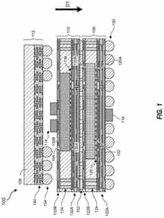
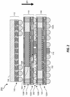
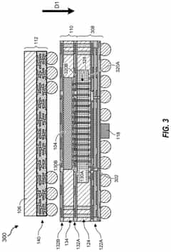
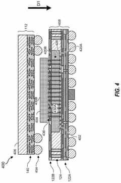
3D chiplet integration using fan-out wafer-level packaging
PatentPendingUS20240274587A1
Innovation
- The use of fan-out wafer-level packaging and three-dimensional packaging techniques for combining semiconductor chips and embedded memory in configurations such as face-to-back, back-to-back, and face-to-face orientations, enabling direct connections between chiplets and reducing assembly package sizes and manufacturing complexity.
FPGA based platform for post-silicon validation of chiplets
PatentPendingUS20230401130A1
Innovation
- A technique is described to facilitate post-silicon validation of a GCD chiplet by enabling it to interface with an FPGA platform, which allows communication with a virtual simulated intellectual property (IP) core, configuring, enumerating, booting, and managing traffic between test silicon and a host test device.


Chiplet Standardization Efforts
Chiplet standardization efforts have become a crucial aspect of the evolving processor architecture landscape. As the industry moves towards disaggregated chip designs, the need for common interfaces and protocols has become increasingly apparent. Several industry consortia and organizations have emerged to address this challenge, working towards establishing standards that will enable seamless integration of chiplets from different vendors.
One of the most prominent initiatives in this space is the Universal Chiplet Interconnect Express (UCIe) consortium. Launched in 2022, UCIe brings together major players in the semiconductor industry, including Intel, AMD, Arm, TSMC, and Samsung. The consortium aims to develop an open industry standard for die-to-die interconnects, focusing on physical and protocol layer specifications. This standardization effort is expected to facilitate interoperability between chiplets from different manufacturers, potentially revolutionizing the way processors are designed and manufactured.
Another significant standardization effort is the Open Compute Project's (OCP) Chiplet Design Exchange (CDX) initiative. CDX focuses on creating a standardized format for exchanging chiplet design information between different tools and organizations. This effort aims to streamline the chiplet design process and enable more efficient collaboration between chiplet providers and system integrators.
The CHIPS Alliance, an open-source hardware organization, has also been actively working on chiplet standardization. Their efforts include developing open-source tools and methodologies for chiplet-based designs, as well as promoting the adoption of open standards in the chiplet ecosystem.
In addition to these industry-wide initiatives, individual companies are also contributing to standardization efforts. For instance, Intel has been promoting its Advanced Interface Bus (AIB) as an open standard for chiplet interconnects. Similarly, AMD has been advocating for its Infinity Fabric technology as a potential industry standard.
These standardization efforts are crucial for the widespread adoption of chiplet-based architectures. By establishing common interfaces and protocols, they aim to reduce design complexity, lower costs, and accelerate time-to-market for chiplet-based products. Furthermore, standardization is expected to foster innovation by enabling a more diverse ecosystem of chiplet providers and system integrators.
However, challenges remain in achieving full industry-wide standardization. Different companies may have conflicting interests, and existing proprietary technologies may hinder the adoption of new standards. Nonetheless, the momentum behind chiplet standardization efforts continues to grow, driven by the potential benefits of a more modular and flexible approach to processor design.
Thermal Management in Chiplet Design
Thermal management has become a critical challenge in chiplet design as the integration of multiple dies on a single package increases power density and heat generation. The modular nature of chiplets introduces unique thermal considerations that must be addressed to ensure optimal performance and reliability. One of the primary concerns is the thermal coupling between adjacent chiplets, which can lead to hotspots and uneven temperature distribution across the package.
To mitigate these issues, designers are implementing advanced cooling solutions tailored specifically for chiplet architectures. These include the use of high-performance thermal interface materials (TIMs) to improve heat transfer between chiplets and the package substrate. Novel TIM formulations, such as those incorporating nanoparticles or phase-change materials, are being developed to enhance thermal conductivity and reduce thermal resistance at interfaces.
Another approach to thermal management in chiplet designs involves the strategic placement of chiplets within the package. By optimizing the layout based on thermal simulations, designers can minimize hotspots and improve overall heat dissipation. This may include positioning high-power chiplets near the edges of the package for better access to cooling solutions or interleaving them with lower-power chiplets to distribute heat more evenly.
Advanced packaging technologies are also playing a crucial role in thermal management for chiplets. Through-silicon vias (TSVs) and interposers can be leveraged not only for electrical connections but also as thermal conduits to efficiently channel heat away from the chiplets. Some designs incorporate dedicated thermal TSVs or micro-fluidic channels within the interposer to enhance cooling capabilities.
Active cooling solutions are being adapted for chiplet-based systems as well. Liquid cooling techniques, such as direct-to-chip liquid cooling or two-phase immersion cooling, are being explored to handle the increased thermal loads of high-performance chiplet designs. These solutions offer the potential for significantly improved heat dissipation compared to traditional air cooling methods.
Furthermore, thermal-aware design methodologies are becoming increasingly important in chiplet integration. This involves considering thermal constraints throughout the design process, from architectural decisions to physical implementation. Advanced thermal modeling and simulation tools are being developed to accurately predict heat distribution in complex chiplet configurations, enabling designers to optimize thermal performance before fabrication.
Unlock deeper insights with PatSnap Eureka Quick Research — get a full tech report to explore trends and direct your research. Try now!
Generate Your Research Report Instantly with AI Agent
Supercharge your innovation with PatSnap Eureka AI Agent Platform!