Comparative Analysis of Microinjection Molding vs Microfabrication
OCT 15, 202510 MIN READ
Generate Your Research Report Instantly with AI Agent
Patsnap Eureka helps you evaluate technical feasibility & market potential.
Micromanufacturing Evolution and Objectives
Micromanufacturing has undergone significant evolution over the past few decades, transforming from experimental laboratory techniques to established industrial processes. The journey began in the 1980s with the emergence of MEMS (Micro-Electro-Mechanical Systems) technology, which laid the foundation for miniaturized manufacturing. By the 1990s, microinjection molding emerged as a specialized adaptation of conventional injection molding, enabling the mass production of microscale plastic components with unprecedented precision.
The parallel development of microfabrication techniques, primarily driven by the semiconductor industry, has created a rich ecosystem of complementary manufacturing approaches. These technologies have evolved from simple photolithographic processes to complex multi-step fabrication sequences incorporating etching, deposition, and surface modification techniques. This technological convergence has enabled the production of increasingly sophisticated microcomponents with feature sizes approaching the nanoscale.
Current technological trends indicate a continued push toward hybrid manufacturing approaches that combine the strengths of both microinjection molding and microfabrication. The integration of these technologies aims to overcome the inherent limitations of each individual process while capitalizing on their respective advantages. This synergistic approach represents a promising direction for addressing complex manufacturing challenges in emerging applications.
The primary objectives of modern micromanufacturing research focus on several key areas. First, enhancing process capabilities to achieve smaller feature sizes while maintaining high aspect ratios and complex geometries. Second, improving production efficiency through increased automation, reduced cycle times, and minimized material waste. Third, expanding material compatibility to include advanced polymers, ceramics, metals, and composite materials with specialized properties.
Additionally, researchers aim to develop more sustainable manufacturing processes by reducing energy consumption, minimizing the use of hazardous chemicals, and exploring bio-based and biodegradable materials. The integration of real-time process monitoring and quality control systems represents another critical objective, enabling adaptive manufacturing processes that can self-correct based on feedback data.
Looking forward, the field is moving toward the concept of "digital micromanufacturing," where computational modeling, simulation, and artificial intelligence guide process optimization and enable predictive quality control. This approach promises to revolutionize how microscale components are designed and manufactured, potentially leading to entirely new classes of products with unprecedented functionality and performance characteristics.
Market Applications and Demand Analysis
The market for micromanufacturing technologies has experienced significant growth over the past decade, driven primarily by increasing demand for miniaturized components across multiple industries. Microinjection molding and microfabrication represent two distinct approaches to producing microscale parts, each serving different market segments with varying requirements and applications.
In the medical device sector, the demand for microinjection molded components has surged due to the growing prevalence of minimally invasive surgical procedures. These procedures require precision components such as catheters, implants, and drug delivery systems. The global medical microinjection molding market segment alone was valued at approximately $1.2 billion in 2022, with projections indicating continued growth at a compound annual rate of 11.3% through 2028.
The electronics industry represents another significant market driver, particularly for microfabrication technologies. With the continuous miniaturization of electronic devices, manufacturers require increasingly precise microcomponents for smartphones, wearables, and IoT devices. The semiconductor industry specifically relies heavily on microfabrication for producing integrated circuits and microelectromechanical systems (MEMS).
Automotive applications have emerged as a rapidly expanding market for both technologies. Modern vehicles incorporate numerous microsensors and control systems that require either microinjection molded parts or microfabricated components. This sector's demand is expected to grow substantially with the increasing adoption of electric and autonomous vehicles, which require even more sophisticated sensing and control systems.
The aerospace and defense industries have shown particular interest in microfabrication technologies for developing advanced sensing systems, communication devices, and specialized components for aircraft and satellites. These applications typically demand the highest precision and reliability, often justifying the higher costs associated with certain microfabrication processes.
Consumer product manufacturers have increasingly adopted microinjection molding for producing components in products ranging from personal electronics to household appliances. The ability to mass-produce complex microparts cost-effectively has opened new design possibilities for consumer goods manufacturers.
Regional market analysis reveals that North America and Europe currently lead in adopting advanced micromanufacturing technologies, particularly in medical and aerospace applications. However, the Asia-Pacific region is experiencing the fastest growth rate, driven by electronics manufacturing and increasing investment in medical device production capabilities.
Market research indicates that customers increasingly prioritize suppliers who can offer integrated solutions combining both microinjection molding and microfabrication capabilities, suggesting a trend toward technological convergence in response to complex manufacturing requirements.
Current Capabilities and Technical Barriers
Microinjection molding and microfabrication represent two distinct approaches to producing microscale components, each with its own set of capabilities and limitations. Currently, microinjection molding can achieve feature sizes down to approximately 10 micrometers with aspect ratios up to 10:1 under optimal conditions. The technology excels in mass production scenarios, with cycle times as short as 5-15 seconds per part, making it highly cost-effective for high-volume manufacturing. Material versatility is another strength, with capabilities to process over 30 different thermoplastics, thermoplastic elastomers, and even ceramic or metal-filled polymers.
In contrast, microfabrication techniques such as photolithography can produce features as small as 0.1 micrometers, offering superior resolution compared to microinjection molding. Silicon-based microfabrication processes have matured significantly, with established protocols for creating complex microelectromechanical systems (MEMS) and integrated circuits. Recent advances in 3D printing at the microscale have also expanded the capabilities of additive microfabrication, though throughput remains significantly lower than injection molding.
Despite these capabilities, both technologies face substantial technical barriers. For microinjection molding, the primary challenges include mold fabrication limitations, where creating high-precision micro-features in mold inserts remains costly and time-consuming. The physics of polymer flow at the microscale introduces unpredictable shrinkage and warpage, with variations often exceeding 5% in critical dimensions. Additionally, demolding microscale features without damage presents significant difficulties, particularly for high aspect ratio structures.
Microfabrication techniques encounter different obstacles, notably material constraints. While microinjection molding can utilize numerous polymers, microfabrication has traditionally been limited to silicon, glass, and a narrow range of metals and polymers. The multi-step nature of many microfabrication processes also introduces cumulative errors and yield issues, with complex devices often experiencing yield rates below 70%. Equipment costs represent another significant barrier, with specialized cleanroom facilities requiring investments of tens of millions of dollars.
Integration challenges exist for both technologies when attempting to combine electrical, mechanical, and fluidic functionalities in a single device. Microinjection molding struggles with embedding electronic components, while microfabrication faces difficulties in creating truly three-dimensional structures with varying material properties. These limitations have spurred research into hybrid manufacturing approaches that combine the strengths of both methodologies.
Recent technological developments are gradually addressing these barriers, with advances in simulation software improving flow prediction in microinjection molding and new coating technologies enhancing mold release properties. Similarly, microfabrication is benefiting from new materials and process innovations that expand its application range beyond traditional semiconductor applications.
Comparative Technical Solutions Assessment
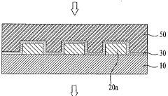
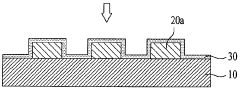
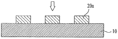
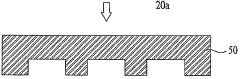
01 Micro-injection molding techniques and equipment
Micro-injection molding involves specialized equipment and techniques for producing microscale components with high precision. This process requires carefully controlled parameters including temperature, pressure, and cooling rates to achieve the desired microstructures. Advanced micro-injection molding systems incorporate precision molds, specialized injection units, and automated handling systems to ensure consistent quality in the production of micro-components.- Microinjection molding techniques and equipment: Microinjection molding involves specialized equipment and techniques for producing microscale components with high precision. These techniques include optimized injection parameters, specialized mold designs, and advanced control systems to achieve micro-features with high accuracy. The process allows for mass production of microparts with complex geometries while maintaining tight tolerances and surface quality required for microdevices.
- Materials for microinjection molding: Various materials are used in microinjection molding, including specialized polymers, composites, and biocompatible materials. These materials are selected based on their flow properties, shrinkage characteristics, and final application requirements. Advanced material formulations enable improved replication of micro-features, enhanced mechanical properties, and compatibility with specific applications such as medical devices or optical components.
- Microfabrication for biomedical applications: Microfabrication techniques are extensively used in biomedical applications, including the production of microfluidic devices, biosensors, and drug delivery systems. These techniques enable the creation of precise microstructures for cell culture, tissue engineering, and diagnostic platforms. The integration of microinjection molding with other fabrication methods allows for the development of complex biomedical devices with enhanced functionality.
- Hybrid and multi-material microfabrication: Hybrid microfabrication combines multiple manufacturing processes to create complex microdevices with integrated functionalities. These approaches include the combination of microinjection molding with other techniques such as laser processing, etching, or additive manufacturing. Multi-material microfabrication enables the production of components with different material properties in a single part, allowing for enhanced performance and functionality in microdevices.
- Precision and quality control in microfabrication: Achieving high precision and quality control in microfabrication requires specialized monitoring systems, process optimization, and advanced inspection methods. These include in-line quality control, optical measurement techniques, and statistical process control adapted for microscale features. The development of standardized testing protocols and metrology solutions ensures the reliability and reproducibility of microinjection molded parts across various applications.
02 Materials for micro-injection molding
Various materials are used in micro-injection molding, including specialized polymers, composites, and biodegradable materials. These materials are selected based on their flow properties, shrinkage characteristics, and final mechanical properties. Advanced material formulations can enhance the replication accuracy of microstructures and improve the performance of the final micro-components. Material selection is critical for achieving the desired surface finish, dimensional accuracy, and functional properties in microfabricated parts.Expand Specific Solutions03 Microfabrication for biomedical applications
Microfabrication techniques are extensively used in biomedical applications, including the production of microfluidic devices, biosensors, and drug delivery systems. These techniques enable the creation of precise microstructures that can interact with biological systems at the cellular level. Biocompatible materials and specialized surface treatments are employed to ensure compatibility with biological samples and living tissues. The integration of microfabricated components into medical devices has led to advancements in diagnostic and therapeutic technologies.Expand Specific Solutions04 Optical and electronic microfabrication
Microfabrication techniques are used to produce optical and electronic components with microscale features. These include micro-lenses, waveguides, microelectronic circuits, and sensors. The processes involve precise replication of microstructures with optical or electronic functionality. Advanced techniques such as multi-material molding and in-mold assembly enable the integration of different functional elements within a single component. These microfabricated optical and electronic components are essential for miniaturized devices in various industries.Expand Specific Solutions05 Innovative mold designs and surface treatments
Advanced mold designs and surface treatments are crucial for successful micro-injection molding and microfabrication. Innovative mold designs incorporate features such as conformal cooling channels, vacuum venting systems, and precise alignment mechanisms. Surface treatments such as coatings, texturing, and nano-structuring enhance the demolding process and improve the replication quality of microstructures. These advancements in mold technology enable the production of increasingly complex and precise micro-components with enhanced functional properties.Expand Specific Solutions
Industry Leaders and Competitive Landscape
Microinjection molding and microfabrication technologies are currently in a mature growth phase, with the global market estimated at $12-15 billion and expanding at 7-9% annually. The competitive landscape features academic institutions (Jiangsu University, Sichuan University) focusing on fundamental research, while established corporations (LG Electronics, Canon, Hon Hai Precision) drive commercial applications. Technology maturity varies by application: microinjection molding excels in high-volume production with companies like Gerresheimer and Taurus Armas leading implementation, while microfabrication dominates in semiconductor applications with Molecular Imprints and Microsoft Technology Licensing holding key patents. The convergence of these technologies is creating new opportunities in medical devices and electronics, with companies like Koninklijke Philips and CGN Juner developing hybrid approaches that leverage advantages of both methodologies.
Molecular Imprints, Inc.
Technical Solution: Molecular Imprints has pioneered advanced microfabrication techniques through their proprietary Jet and Flash Imprint Lithography (J-FIL) technology, which bridges the gap between traditional microfabrication and microinjection molding. Their approach utilizes a low-viscosity photocurable material dispensed in droplet form onto substrates, followed by imprinting with a patterned template and UV curing. This process achieves sub-10nm resolution features while maintaining high throughput capabilities. The company has developed specialized equipment that enables precise control over material dispensing, template alignment, and separation processes, allowing for consistent pattern replication across large areas. Their technology has been particularly successful in semiconductor applications, where they've demonstrated the ability to create complex 3D microstructures with significantly reduced process steps compared to conventional lithography methods.
Strengths: Achieves extremely high resolution (sub-10nm) with excellent pattern fidelity; offers lower cost per part for high-volume production; reduces material waste compared to traditional methods. Weaknesses: Requires specialized equipment with high initial capital investment; template fabrication can be complex and expensive; limited material selection compared to microinjection molding.
The Georgia Tech Research Corp.
Technical Solution: Georgia Tech Research Corporation has developed a hybrid approach that combines the advantages of both microinjection molding and microfabrication techniques. Their technology utilizes a two-stage process where microfabrication methods (primarily photolithography and etching) are first employed to create high-precision master molds, which are then used for subsequent microinjection molding. This approach leverages Georgia Tech's expertise in microfluidics and MEMS (Micro-Electro-Mechanical Systems) fabrication. Their research has focused on developing specialized surface treatments for molds that enhance demolding capabilities while maintaining nanoscale feature fidelity. Additionally, they've pioneered techniques for creating hierarchical structures with both micro and nano features simultaneously, which has applications in biomedical devices, optical components, and microfluidic systems. Their process innovations have demonstrated the ability to produce complex 3D microstructures with aspect ratios exceeding 20:1 while maintaining sub-micron precision.
Strengths: Combines precision of microfabrication with throughput advantages of injection molding; enables complex hierarchical structures; suitable for both prototyping and mass production. Weaknesses: Process chain complexity increases production time; requires expertise in both fabrication domains; higher initial development costs compared to single-technology approaches.
Critical Patents and Research Breakthroughs
Method for manufacturing a master mold which is used to form a micropatterned film applied to an exterior of a household appliance and manufacturing apparatus and method of the film using the master mold
PatentWO2011028060A2
Innovation
- A method involving the use of a stainless steel substrate with photoresist application, UV irradiation, and wet etching to create a master mold, which can then replicate micropatterns onto synthetic resin substrates, allowing for the production of micropatterned films that can be applied to household appliances with varying sizes and designs at a lower cost.
Polymer micro-cantilever with probe tip and method for making same
PatentInactiveUS20070237676A1
Innovation
- The development of micro-cantilevers made from thermoplastic polymers using injection molding techniques, which allows for the production of cantilevers with tunable mechanical properties and integrated probe tips, enabling more sensitive and cost-effective detection of molecular interactions.
Material Science Considerations
Material selection represents a critical differentiating factor between microinjection molding and microfabrication processes. Microinjection molding predominantly utilizes thermoplastic polymers such as polyoxymethylene (POM), polycarbonate (PC), polyamide (PA), and liquid crystal polymers (LCP). These materials offer advantages including excellent flow properties at processing temperatures, rapid solidification rates, and dimensional stability upon cooling. The material science considerations for microinjection molding focus on rheological behavior under high shear rates and the polymer's ability to fill microscale features completely.
In contrast, microfabrication techniques accommodate a broader spectrum of materials including silicon, glass, metals, ceramics, and specialized polymers. Silicon remains the dominant substrate in MEMS (Micro-Electro-Mechanical Systems) applications due to its well-established processing protocols and excellent mechanical properties at the microscale. The crystalline structure and anisotropic etching characteristics of silicon enable precise feature creation through techniques like deep reactive ion etching (DRIE).
Material compatibility with processing conditions presents unique challenges for both approaches. In microinjection molding, polymer degradation can occur due to excessive shear heating or residence time in the barrel. Additionally, the high cooling rates experienced in micro-molds can induce significant residual stresses, affecting part performance and dimensional accuracy. Material additives such as nucleating agents and flow enhancers are frequently incorporated to improve processability and final part properties.
For microfabrication, material considerations extend to chemical compatibility with etching solutions, photoresist adhesion properties, and thermal stability during deposition processes. The layered nature of many microfabrication techniques necessitates careful management of interfacial stresses between dissimilar materials, particularly when thermal cycling is involved during processing.
Recent advances in material science have expanded the capabilities of both technologies. For microinjection molding, the development of specialized micro-compounds with enhanced flow properties and reduced viscosity has enabled the production of increasingly complex microstructures. Similarly, microfabrication has benefited from new photoresist formulations and the integration of novel materials like shape memory alloys and piezoelectric compounds, broadening the functional capabilities of microfabricated devices.
Surface properties and material-specific characteristics significantly influence the selection between these manufacturing approaches. Microinjection molding excels in producing parts with consistent bulk properties, while microfabrication offers superior control over surface chemistry and topography at the nanoscale. This distinction becomes particularly important in applications requiring specific surface interactions, such as microfluidic devices or biosensors.
Cost-Efficiency and Scalability Analysis
When comparing microinjection molding and microfabrication technologies from a cost-efficiency and scalability perspective, several critical factors emerge that influence industrial adoption and implementation strategies.
Microinjection molding demonstrates significant cost advantages in high-volume production scenarios. The initial tooling costs, while substantial ($10,000-$100,000 depending on complexity), are effectively amortized across large production runs. Once the mold is created, the marginal cost per part drops dramatically, often to mere cents per unit. This creates a compelling economic model for mass production, with break-even points typically occurring between 10,000 and 100,000 units depending on part complexity.
Microfabrication technologies, particularly those based on semiconductor processing techniques, present a different cost structure. These methods typically involve higher operational costs due to clean room requirements, specialized equipment, and more complex multi-step processes. The per-unit costs remain relatively stable regardless of volume, making them less economically favorable for mass production but potentially more cost-effective for low-volume, high-value applications such as medical diagnostics or specialized research tools.
Scalability considerations reveal distinct advantages for each technology. Microinjection molding excels in scaling production volume, with cycle times as short as 5-15 seconds per part and the ability to incorporate multi-cavity molds that can produce multiple parts simultaneously. Modern automated systems can achieve production rates exceeding 100,000 parts per day with minimal human intervention, representing exceptional throughput efficiency.
Microfabrication offers superior scalability in terms of design complexity and feature miniaturization. Techniques like photolithography can consistently produce features at the sub-micron scale across large substrate areas, enabling complex integrated systems on a single substrate. This "scaling down" capability allows for increasingly sophisticated functionality within the same footprint, though production throughput remains limited compared to injection molding.
Material considerations also impact cost-efficiency. Microinjection molding can utilize a wide range of thermoplastics costing $2-20 per kilogram, while specialized materials for microfabrication often cost significantly more. However, microfabrication typically uses less material per device, potentially offsetting some of this cost differential in certain applications.
Recent market analysis indicates that industries requiring millions of identical microparts with moderate complexity increasingly favor microinjection molding, with annual growth rates of 8-12% in this sector. Conversely, applications requiring extreme precision or integrated functionality continue to rely on microfabrication despite higher unit costs, particularly in emerging fields like organ-on-chip technology and advanced biosensors.
Unlock deeper insights with Patsnap Eureka Quick Research — get a full tech report to explore trends and direct your research. Try now!
Generate Your Research Report Instantly with AI Agent
Supercharge your innovation with Patsnap Eureka AI Agent Platform!